That is, when the thin film circuit is deposited by means of the
sputtering or the like, the surface properties of a thin film surface (circuit surface) are important; when there is an unevenness on the surface, the circuit is deposited with deteriorated accuracy.
In particular, in the aluminum nitride sintered body, when the heat dissipation properties are improved, there is a tendency in that a
sintering additive, which forms a
liquid phase that may deteriorate the
thermal conductivity, is added less.
In case the sintering additive is added less, when a sintering temperature is not raised high enough, sintering characteristics deteriorate.
Furthermore, when there are excessively grown aluminum nitride
crystal grains on the
substrate surface, since flatness on the
substrate surface is deteriorated, it becomes difficult to uniformly deposit a thin film.
In the existing aluminum nitride sintered body, during the mirror polish or acid wash, the
grain boundary phase component present on the surface of the sintered body is likely to fall off or be dissolved.
Accordingly, there is a problem in that the thin film is difficult to deposit with high accuracy.
These may cause a relatively large pit.
The space between the thin film and the aluminum nitride substrate may cause swelling due to heat applied in the later course of manufacture and during the use of the circuit, resulting in lowering the circuit accuracy or in peeling the thin film.
However, simple control of the
polishing conditions of the aluminum nitride sintered body may not necessarily sufficiently satisfy the characteristics demanded for the thin film surface.
However, as mentioned above, since, in the thin film substrate, the surface state may cause problems, simple control of an amount of the
grain boundary phase inside the sintered body may not sufficiently satisfy the characteristics demanded for the thin film surface.
In particular, in the aluminum nitride sintered body, in which high
thermal conductivity is intended, since the grain boundary phase tends to precipitate on the sintered
body surface, simple control of the amount of the grain boundary phase inside of the sintered body may adversely affect on the surface characteristics.
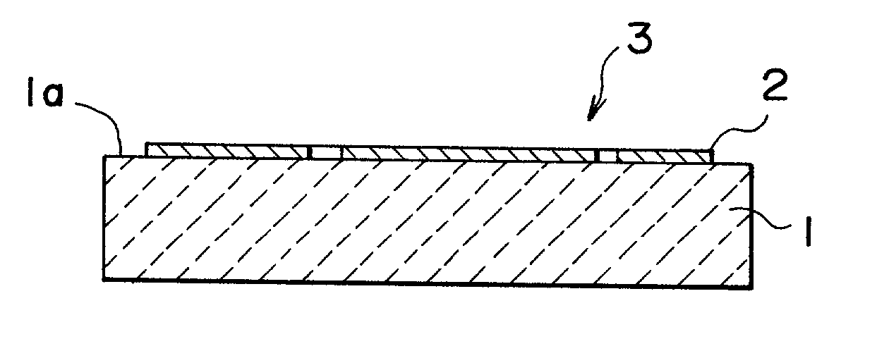
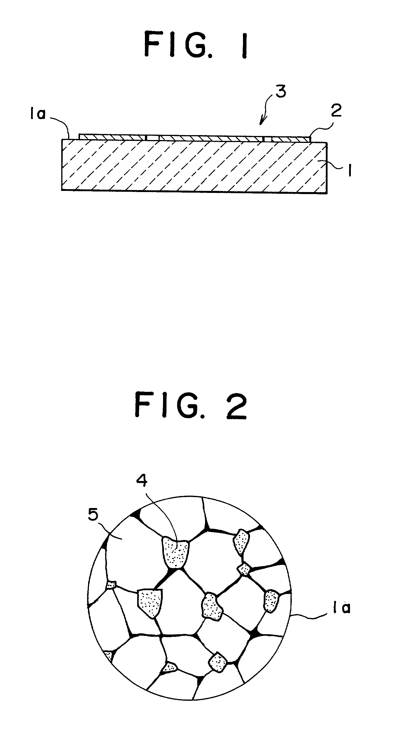
As a result, advantages due to the use of the AlN substrate 1 may be damaged.
On the other hand, when the
rare earth oxide is compounded less than 1% by
mass, sintering characteristics of the AlN sintered body or the like may be deteriorated to result in an increase of the pore or a decrease of the
thermal conductivity.
In particular, since the compound, which constitutes the aforementioned grain boundary phase, is easily dissolved by an acid, the
dissolution of the aggregate 4 in the course of the acid wash after the mirror finish may cause a large pit (
cave).
These may cause accuracy deterioration or peel in the circuit formed with the
metal thin film 2.
on the other hand, when the skewness Rsk of the mirror finished surface exceeds 1 (Rsk>1), as a whole, there are too many upward peaks; in such cases also, the circuit deposition accuracy due to the
metal thin film 2 deteriorates.
On the other hand, when the average grain size of the AlN
crystal grains is less than 3 .mu.m, thermal
conductivity of the AlN sintered body remarkably decreases; thermal
conductivity of, for instance, 160 W / m K at
room temperature may not be satisfied.
This causes characteristics deterioration of the thin film substrate 3.
Similarly, when the
impurity oxygen concentration exceeds 1% by
mass, the AlN
crystal grain may unnecessarily grow larger, and the thermal
conductivity of the AlN sintered body deteriorates.
The dispersion process may be performed exceeding 3 hr, but a further effect may not be obtained by the longer dispersion time, resulting in only prolonging the manufacturing time.
Simple
miniaturization of the crystal grain size may remarkably decrease the thermal conductivity of the AlN sintered body.
That is, when the skewness Rsk of the surface after the semi-finish due to the
diamond abrasive is smaller than -1 (Rsk<-1), whatever the mirror finishing conditions after that may are controlled, the
surface roughness of the mirror finished surface may not satisfy the desired value.

