Etchant, etching method and semiconductor silicon waffer

a technology of semiconductor silicon and etching method, which is applied in the direction of crystal growth process, after-treatment details, inorganic non-surface-active detergent composition, etc., can solve the problems of mechanical strength, adversely affecting electrical characteristics, and needing to be removed completely

Inactive Publication Date: 2003-01-09
SHIN-ETSU HANDOTAI CO LTD
View PDF1 Cites 11 Cited by
  • Summary
  • Abstract
  • Description
  • Claims
  • Application Information

AI Technical Summary

Benefits of technology

0008] According to a first aspect of the present invention, an etchant of the present invention is prepared by immersing stainless steel in an alkali aqueous solution for not less than 10 hours. Metallic elements dissolved in such etchant are extremely reduced.

Problems solved by technology

In a manufacturing process of devices, since the process damage layer induces a crystal defect, such as slip dislocation, lowers mechanical strength of a wafer, and also affects adversely on electrical characteristic, it is required to be removed completely.
Therefore, as a material of an etching vessel, for example, even if it is the case that polypropylene is used in consideration of corrosion resistance, the silicon wafer is contaminated by the iron, nickel, chromium, and copper or the like, which are included in the alkali aqueous solution.
However, even by these methods, the amount of contamination of the metallic elements adhering to or being diffused inside an etched wafer, is still a problem for manufacturing the latest high integration device.

Method used


Image

  • Etchant, etching method and semiconductor silicon waffer
  • Etchant, etching method and semiconductor silicon waffer
  • Etchant, etching method and semiconductor silicon waffer

Examples


experiment 1

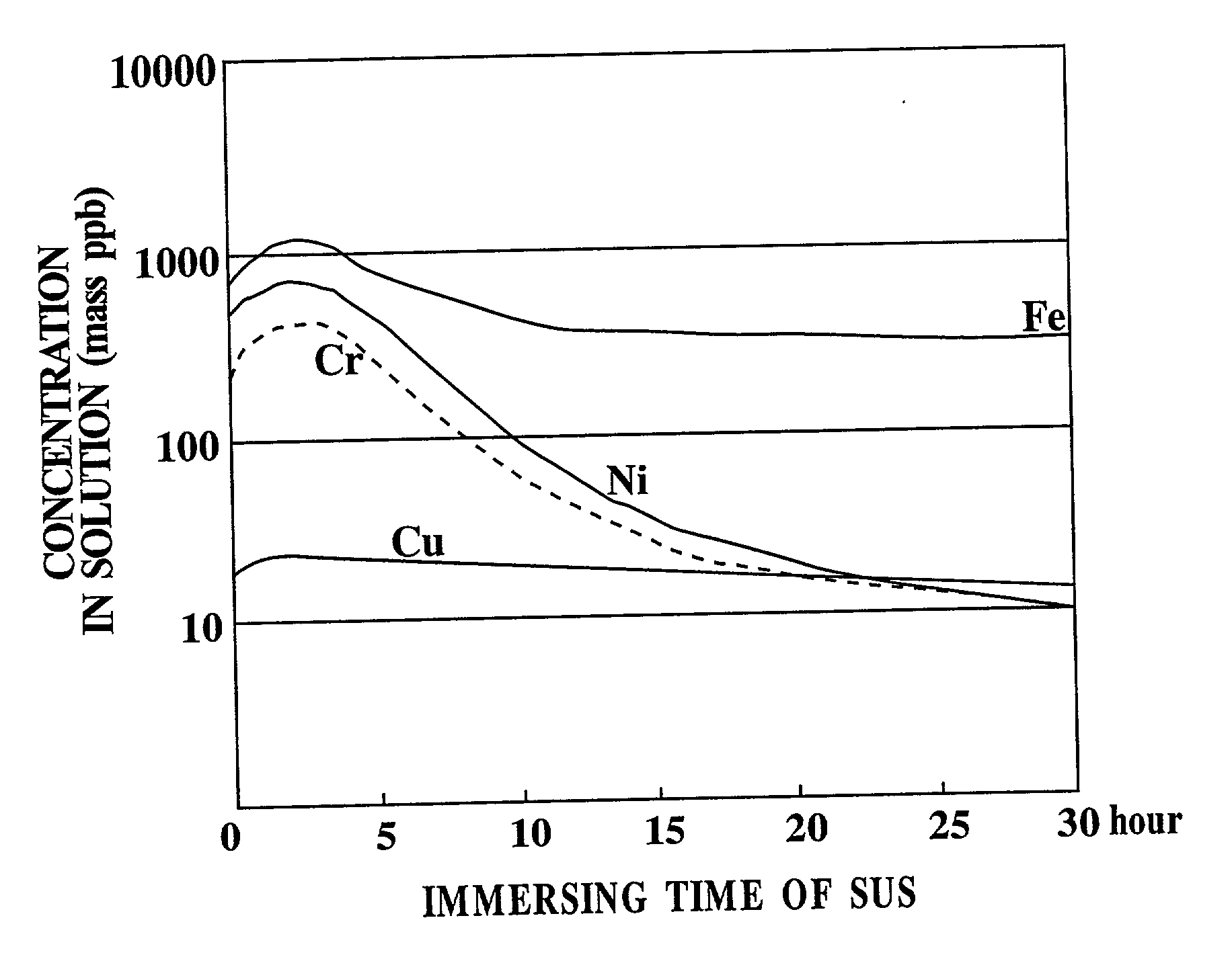
[0049] The effect of reduction of metal ion concentrations in an etchant by immersion of SUS, was studied. That is, the immersing time of SUS for immersing in a sodium hydroxide aqueous solution was made into 2, 4, 8, 10, 12, 15, 20 and 30 hours, respectively. Then, the concentrations of Fe, Ni, Cr, and Cu ions in each sodium hydroxide aqueous solution to which the SUS immersing treatment was made, were measured. The results are shown in FIG. 1.

[0050] As shown in FIG. 1, when the immersing time of SUS is at least 10 hours, preferably, 12 hours or more, it is known that the reducing effect of concentrations of the metal ions in the solution is very remarkable to Fe, Ni, and Cr, and also effective to Cu. When the time is lengthened more than that, the effect is recognized further. However, since the effect is reduced gradually, an appropriate time of 10 hours or more, practically, may be chosen according to need. Therefore, in all of the examples and the comparative examples hereinaft...


PUM

PropertyMeasurementUnit
temperatureaaaaaaaaaa

Abstract

An etchant and an etching method that contribute to prevention of metal contamination of a semiconductor silicon wafer, and a semiconductor silicon wafer in which metal contamination is extremely reduced, are provided. The etchant according to the present invention is prepared by immersing stainless steel in an alkali aqueous solution for not less than 10 hours. In the etching method according to the present invention, a semiconductor silicon wafer is etched by using the etchant. Thereby, the semiconductor silicon wafer according to the present invention, in which metal contamination is extremely reduced, is obtained.

Description

[0001] The present invention relates to a semiconductor material, particularly, to an etchant, an etching method of a silicon wafer, and a semiconductor silicon wafer.[0002] A silicon wafer passed through machining processes of block cutting, outer diameter grinding, slicing, and lapping, has a damaged layer, that is, an process damage layer, on the surface. In a manufacturing process of devices, since the process damage layer induces a crystal defect, such as slip dislocation, lowers mechanical strength of a wafer, and also affects adversely on electrical characteristic, it is required to be removed completely.[0003] Conventionally, removing the process damage layer, which is introduced into a silicon wafer in the machining processes, by chemical etching, is carried out. As methods of the chemical etching, there are acid etching and alkali etching. Among these, the alkali etching has few problems in occurrence of a harmful by-product, such as NO.sub.x in the acid etching, and littl...

Claims


Application Information

Patent Timeline
Patent Type & Authority Applications(United States)
IPC IPC(8): C01D1/28C11D7/06C30B29/06C11D11/00C30B33/08H01L21/306
CPCC01D1/28C11D7/06C11D11/0047H01L21/02019H01L21/30604H01L21/30608H01L21/3063
Inventor MIYAZAKI, SEIICHI
Owner SHIN-ETSU HANDOTAI CO LTD
Why Eureka
Try Eureka