Methods and apparatuses for heat treatment of semiconductor films upon thermally susceptible non-conducting substrates

a technology of non-conducting substrates and heat treatment methods, which is applied in the direction of induction heating, electric/magnetic/electromagnetic heating, furnaces without endless cores, etc., can solve the problems of glass damage or distortion, glass is easily deformed, and requires high thermal budgets, so as to improve the uniformity of the process, and strengthen the magnetic field

Inactive Publication Date: 2003-01-16
KIM HYOUNG JUNE
View PDF6 Cites 36 Cited by
  • Summary
  • Abstract
  • Description
  • Claims
  • Application Information

AI Technical Summary

Benefits of technology

0032] (1) The magnetic core with a plate shape encapsulates the upper portion of pancake-shaped flat induction coil so that external magnetic flux is generated from the magnetic poles downward to the surface of said silicon film located underneath the said induction coil. This configuration yields magnetic flux distribution in close proximity to the non-conducting substrate without being dissipated away. It is desired that the substrate is subjected to linear motion underneath the coil to improve the uniformity of the process.
0033] (2) The magnetic core with horse shoe-shaped (-shape-vertical, cross-sectional view) which is wound by multi-turn induction coil is located above the semiconductor films allowing exposure of external magnetic flux traveling between two magnetic poles to the semiconductor films. In this configuration, the applied current of induction coil produces the strengthened magnetic field through a function of the magnetic core. The magnetic flux then travels directly from one pole to the other across the air gap. It is desired that the non-conducting substrate under heat treatment is subjected to continuous linear movement underneath the coil to improve the uniformity of the process.
003...

Problems solved by technology

Glass is easily deformed when exposed to the temperature above 500.degree. C. for substantial length of time.
Those heat treatments typically require high thermal budgets, unavoidably causing damage or distortion of glass.
However, high thermal budget of this method leads to damage and/or distortion of used glass substrates.
However, this method has critical drawbacks for its use in mass production.
The grain structure of poly-Si film through this process is extremely sensitive to the laser beam energy, so that an uniformity in grain structure and hence the device characteristics can not be achieved Also, the beam size of the laser is relatively small.
Since it is difficult to precisely control the laser, the multiple shots introduce non-uniformities into the crystallization process.
Further, the surface of ELC poly-Si films is rough, which also degrades the device performance.
The ELC also has a problem of hydrogen eruption when deposited amorphous Si has high hydrogen contents, which is usually the case in the plasma enhanced chemical vapor deposition (PECVD).
In addition to the prob...

Method used


Image

  • Methods and apparatuses for heat treatment of semiconductor films upon thermally susceptible non-conducting substrates
  • Methods and apparatuses for heat treatment of semiconductor films upon thermally susceptible non-conducting substrates
  • Methods and apparatuses for heat treatment of semiconductor films upon thermally susceptible non-conducting substrates

Examples


Embodiment Construction

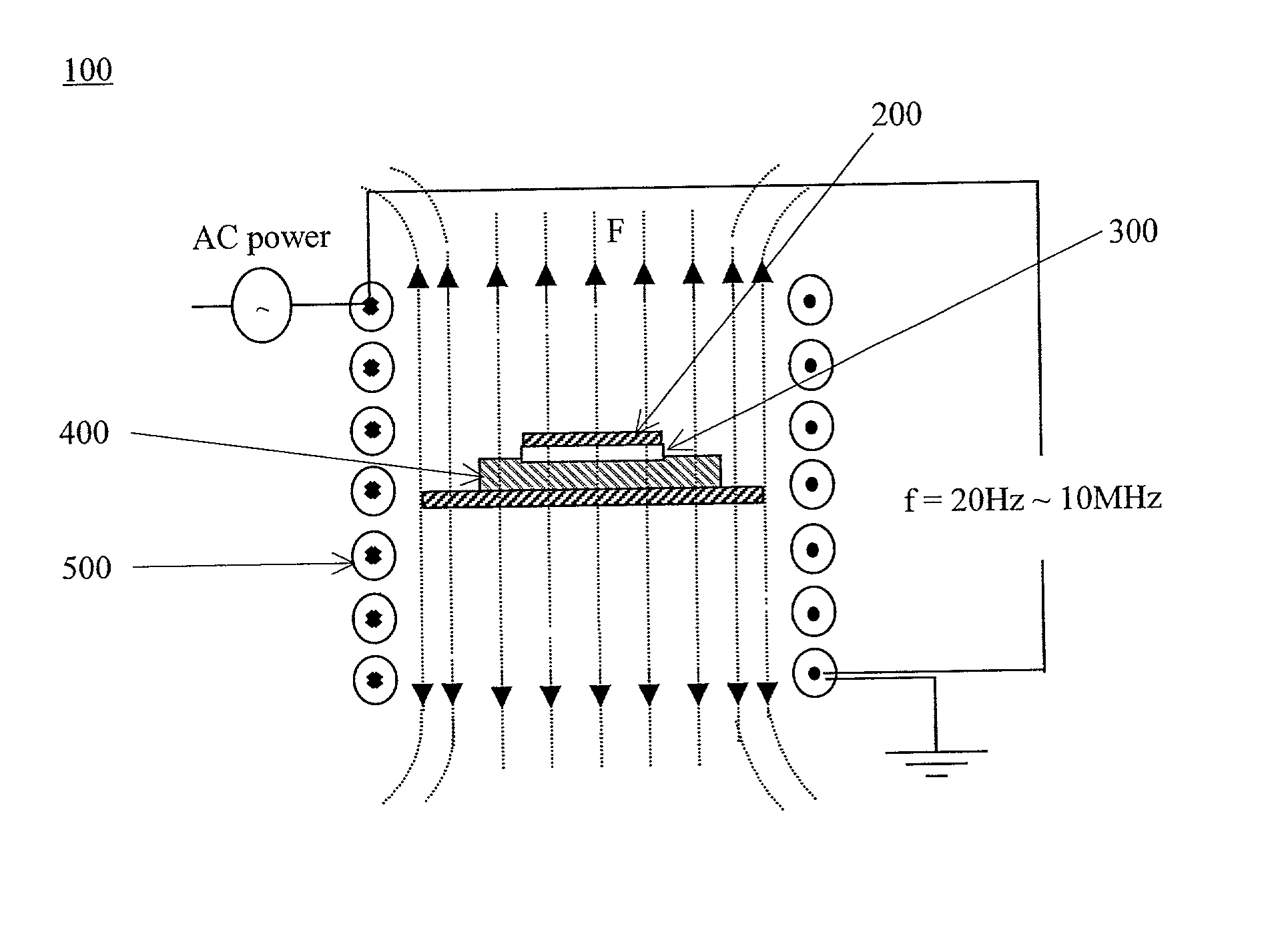
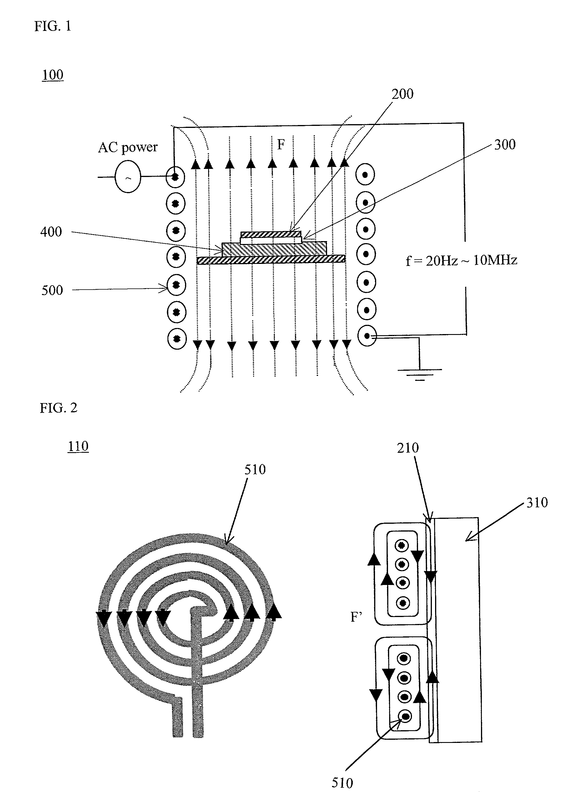
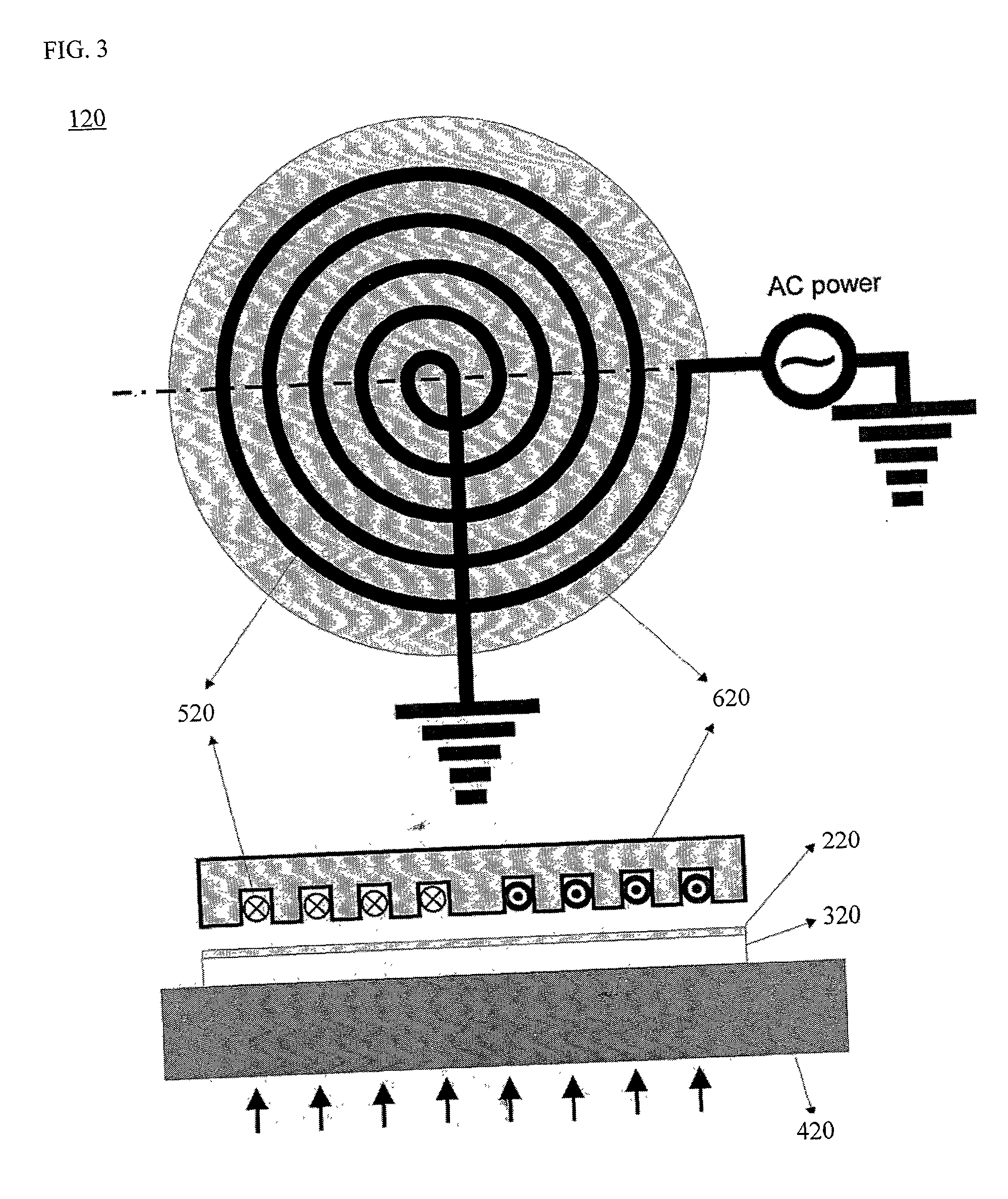
[0057] Referring to FIG. 1, the present embodiment relates to an apparatus allowing low temperature heat treatments of a silicon film on a glass substrate. This apparatus can be used for heat treatments of both crystallization of amorphous silicon and dopant activation of ion-implanted silicon.

[0058] Apparatus 100 consists of a graphite susceptor 400 heating the glass substrate 300 coated with the silicon film 200 and a solenoid induction coil 500 generating magnetic field (F). Introduction of alternating current in the water-cooled induction coil leads to a generation of alternating magnetic field (F). The alternating magnetic flux is utilized for two purposes. First is to heat the graphite susceptor 400 through a function of joule heating effects (i.e., heating mechanism of a conventionally used induction furnace). Second is to enhance the kinetics of heat treatments of silicon films 200 through an inducted emf inside the silicon films 200. In order to see the enhancement effects,...


PUM


Abstract

The present invention relates to methods and apparatuses for heat treatment of semiconductor films upon thermally susceptible non-conducting substrates at a minimum thermal budget are required, and more particularly, to a polycrystalline silicon thin-film transistors (poly-Si TFTs) and PN diodes on glass substrates for various applications of liquid crystal displays (LCDs), organic light emitting diodes (OLEDs), and solar cells. According to the methods and apparatus of the present invention, the semiconductor films can be heat-treated without damaging the thermally susceptible substrates; e.g., crystallization of amorphous silicon films at the minimum thermal budget acceptable for the use of glass, enhancing kinetics of dopant activation at the minimum thermal budget acceptable for the use of glass.

Description

[0001] The present invention relates to methods and apparatuses for heat treatment of semiconductor films upon thermally susceptible non-conducting substrates at a minimum thermal budget. More particularly the invention relates to polycrystalline silicon thin-film transistors (poly-Si TFTs) and PN diodes on glass substrates for various applications of liquid crystal displays (LCDs), organic light emitting diodes (OLEDs), and solar cells.[0002] Liquid crystal displays (LCDs) and organic light emitting diodes (OLEDs) grow rapidly in the flat panel displays. In the present time, those display systems employ the active matrix circuit configuration using TFTs. Fabrication of thin film transistors (TFTs) on glass substrate is necessary in those applications.[0003] TFT-LCDs typically uses the TFTs composing amorphous Si films as an active layer (i.e., a-Si TFT LCD). Recently, interests on the development of TFTs using polycrystahline silicon films instead of amorphous silicon films (i.e., ...

Claims


Application Information

Patent Timeline
IPC IPC(8): H05B6/10H01L21/00H01L21/20H01L21/268H01L21/336H01L29/786
CPCH01L21/67115
Inventor KIM, HYOUNG JUNE
Owner KIM HYOUNG JUNE
Why Eureka
Try Eureka