Electronic component incorporating an integrated circuit and planar microcapacitor

Inactive Publication Date: 2003-07-03
SAKURATECH
View PDF4 Cites 50 Cited by
  • Summary
  • Abstract
  • Description
  • Claims
  • Application Information

AI Technical Summary

Problems solved by technology

Such microcapacitors have the drawback of being limited in their capacitance value.
The risk is then that the proximity of the electrodes would result in undesirable spurious phenomena, by means of the tunnel effect.
The dielectric behaviour of such thin layers must also be mentioned among the drawbacks of such capacitors, since they cause avalanche effects.
Nevertheless, it is noted that a

Method used


Image

  • Electronic component incorporating an integrated circuit and planar microcapacitor
  • Electronic component incorporating an integrated circuit and planar microcapacitor
  • Electronic component incorporating an integrated circuit and planar microcapacitor

Examples


Example

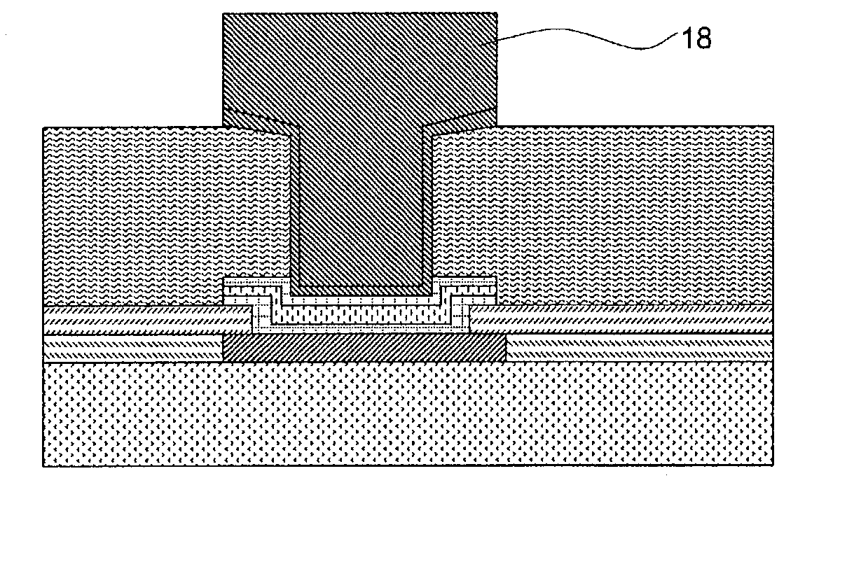
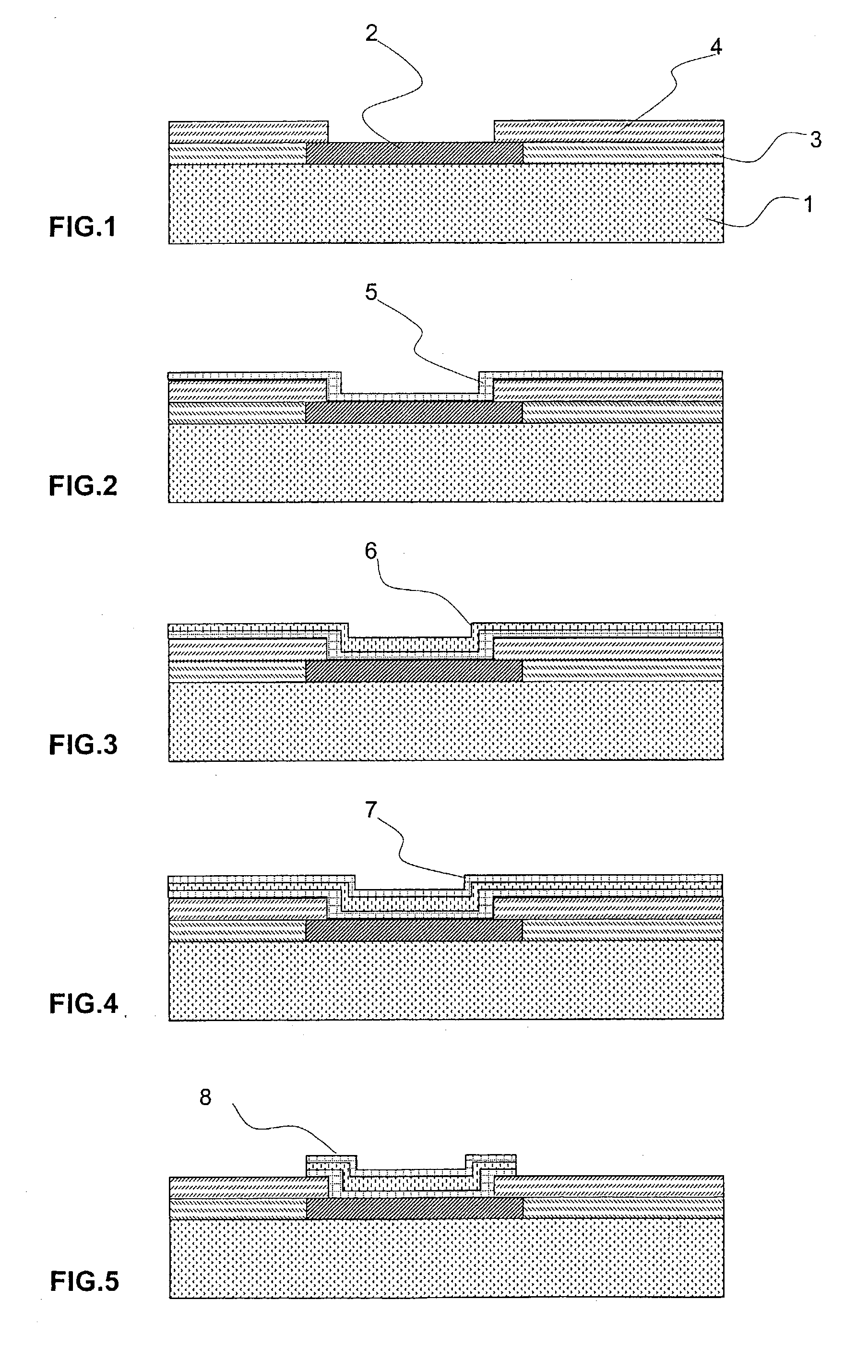
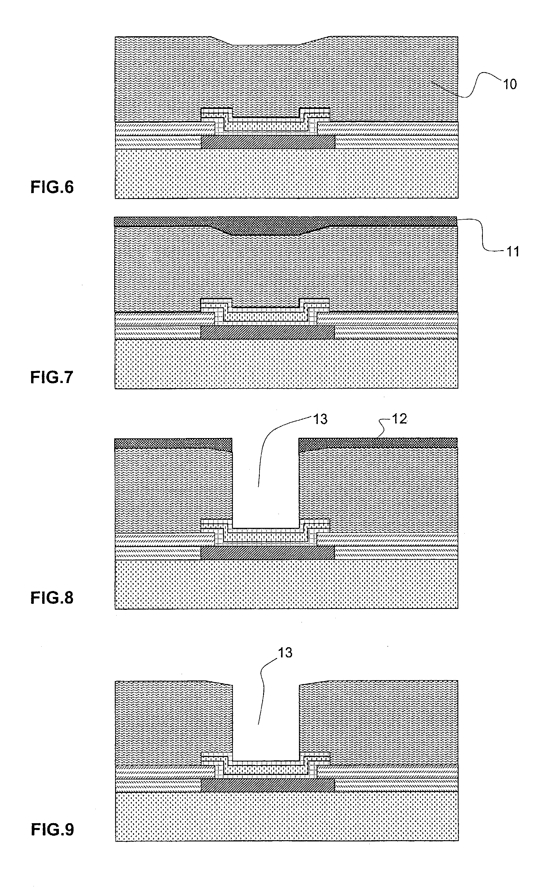
[0031] As already stated, the invention relates to a microcapacitor made on an electronic component incorporating an integrated circuit.

[0032] This capacitor may be made, as in the illustrated figures, in the upper plane of the substrate. Nevertheless, in other forms of embodiment (not illustrated), this microcapacitor may be made within the substrate itself, in the lower metallization plane of the integrated circuit.

[0033] Thus, as illustrated in FIG. 1, the substrate (1) may comprise a connection pad (2) made from a material such as aluminum or copper, or even an aluminum-silicon, aluminum-copper or copper-zinc alloy. In the form illustrated, the substrate (1) is coated with a first passivation layer (3), typically made of SiO.sub.2. This silica layer (3) is coated with a layer of silicon nitride Si.sub.3N.sub.4 making it possible to protect the lower silica layer against exposure to air.

[0034] Before proceeding to deposit the various characteristic layers, non-corrosive cleaning ...


PUM

PropertyMeasurementUnit
Nanoscale particle sizeaaaaaaaaaa

Abstract

Electronic component incorporating an integrated circuit made in a substrate (1) and a planar capacitor, characterized in that the capacitor is made on top of a metallization plane of the component, this metallization plane forming a first electrode (2) of the capacitor, and in that the capacitor comprises: a first oxygen diffusion barrier layer (5) deposited on top of the metallization plane (2); a stack (6) of several different oxide layers, each layer having a thickness less than 100 nanometres, the stack being deposited on top of the first barrier layer (5); a second oxygen diffusion barrier layer (7) deposited on top of the stack of oxide layers (6); a metal electrode (20) present on top of the second barrier layer (7).

Description

[0001] The invention relates to the technical field of microelectronics. More specifically, it relates to an electronic component incorporating a microcapacitor which can be used within the scope of applications, for example radiofrequency applications. This capacitor may be made on the upper face of the substrate of the component, or else inside the substrate itself, at the core of an integrated circuit. The design of such a capacitor makes it possible to obtain particularly high capacitance values.PRIOR ART[0002] The production of microcapacitors on silicon substrates has already been the subject of some development.[0003] Thus, document FR 2 801 425 describes a microcapacitor, the dielectric portion of which consists of two layers of different materials, and more specifically, on the one hand, of silicon dioxide, and on the other hand, of silicon nitride. Such microcapacitors have the drawback of being limited in their capacitance value. This is because the dielectric constants (...

Claims


Application Information

Patent Timeline
IPC IPC(8): H01L27/04C23C16/40C23C16/44C23C16/455H01L21/28H01L21/316H01L21/822H01L29/51
CPCC23C16/40C23C16/45529H01L29/511H01L21/31604H01L21/28167H01L21/02263
Inventor GIRARDIE, LIONEL
Owner SAKURATECH
Why Eureka
Try Eureka