Copper electroplating method using insoluble anode

a technology of copper electroplating and insoluble anode, which is applied in the direction of cell components, printing, transportation and packaging, etc., can solve the problems of deformation or destruction of printed wiring boards, difficulty in filling holes that have a small diameter and are not through holes, and drawbacks to the miniaturization of build-up printed wiring boards. , to achieve the effect of safe and convenient stirring

Inactive Publication Date: 2004-03-18
SHIPLEY CO LLC
View PDF4 Cites 12 Cited by
  • Summary
  • Abstract
  • Description
  • Claims
  • Application Information

AI Technical Summary

Benefits of technology

[0039] The concentration of the sulfuric acid in the copper sulfate plating solution is generally 30 to 400 g / L, preferably 170 to 210 g / L. For example, when a concentration is less than 30 g / L, the conductivity of the plating bath may be too low to produce a current through the plating bath. Further, when a concentration is more than 400 g / L, the dissolution of the copper sulfate may be prevented, which leads to precipitation of the copper sulfate.
[0056] The copper electroplating method of the present invention employs an insoluble anode as an anode, and therefore the decomposition reaction on the sulfur-containing compound described above is prevented from occurring, so that the copper electroplating bath is substantially free of the decomposition products. Accordingly, in the copper electroplating method of the present invention, no void is left in the via filling, and no bulky grain is formed in the metal deposition, so that it is possible to avoid the disadvantages in usage of the sulfur-containing compound a brightener, which has been a problem in the conventional methods. In other words, according to the present invention, the use of the insoluble anode in the copper electroplating substantially eliminates the decomposition products that would otherwise be formed through the cleavage of an S--X or S--Y bond of the sulfur-containing compound, and the bath solution can be controlled to be in conditions suitable for desired copper electroplating.
[0060] In the plating method of the present invention, stirring may safely be carried out. Preferably, stirring is carried out to uniformly supply the copper ions and the additives to the surface of the material to be plated. Aeration or jet can be used for the stirring. Additionally, batch filtration or circulating filtration may be carried out. The plating solution is preferably circulated and filtrated with a filter, so that the temperature of the plating solution can be uniform, and dusts, precipitates, and the like can be removed from the plating solution.
[0061] According to the copper electroplating method of the present invention, a composite material is produced which comprises a substrate and a copper layer formed on the substrate. According to the method of the present invention, even if the copper electroplating process following the initial make-up of the electrolytic bath is interrupted, and the bath is allowed to stand for a certain time period and then used again, the copper layer of the produced composite material can be free of bulky grains, and the via can be filled with no remaining void.

Problems solved by technology

When the resin used in such a process is viscous, it is difficult to fill up a hole that has a small diameter and is not a through hole.
If the MVH space is left partially unfilled after the filling step with the resin, the air remaining in the MVH may be quickly expanded by heat in soldering the printed wiring board, leading to deformation or destruction of the printed wiring board.
In the conventional process, therefore, the diameter of the MVH has to be large enough to facilitate the resin filling, which causes a drawback to the miniaturization of the build-up printed wiring board.
This may reduce the area efficiency and design flexibility of the build-up printed wiring board.
However, since the conductive paste, which is a mixture of copper and an organic material, has a lower conductivity than that of copper metal, the small diameter MVH cannot provide sufficient electrical connection, and therefore the method with the conductive paste can hardly be useful in miniaturizing and increasing the density in the printed wiring board.
However, the method suffers from a low deposition rate and low productivity of the plated coating film.
According to this process, it will take 30 hours or more to fill up a typical MVH of 100 .mu.m in diameter and 100 .mu.m in depth with the plated copper, and the productivity is very low.
Inside the MVH, however, the deposition rate of the conventional copper electroplating is very low, and therefore it has been considered impractical to fill up the MVH by copper electroplating.
The void formed in the copper deposition may cause deformation or destruction of the printed wiring board, because the substances captured in the void (the plating solution or hydrogen gas) may be quickly expanded in soldering on-board parts to the printed wiring board at high temperature.
In the plating process using the soluble anode, however, the copper electroplating bath may become unstable when the electrolysis is interrupted.
If the copper electroplating solution is used after the interruption, bulky grains can be formed in the electroplated copper layer, and formation of the filled via can become unstable.

Method used


Image

  • Copper electroplating method using insoluble anode
  • Copper electroplating method using insoluble anode
  • Copper electroplating method using insoluble anode

Examples


example 1

[0066] Copper Electroplating with Insoluble Anode Conditions for Copper Electroplating Plating Solution:

1 Sulfuric Acid 180 g / L Copper Sulfate 150 g / L Chloride Ion 60 mg / L Surfactant 0.35 g / L Brightener 5 mg / L

[0067] Surfactant: HO--(CH.sub.2--CH.sub.2--O).sub.a--(CH.sub.2--CH(CH.sub-.3)--O).sub.b--(CH.sub.2--CH.sub.2--O).sub.c--H

[0068] (where a+c=25, b=30)

[0069] Brightener: Na--SO.sub.3--(CH.sub.2).sub.3--S--S--(CH.sub.2).sub.3---SO.sub.3--Na

[0070] Current Density: 2 A / dm.sup.2

[0071] Plating Time: 60 minutes

[0072] Cathode: Build-Up Board

[0073] Cathode Area: 1 dm.sup.2

[0074] Anode: Iridium Oxide

[0075] Anode Area: 1 dm.sup.2

example 2

[0086] Copper Electroplating with Insoluble Anode Conditions for Copper Electroplating Plating Solution:

3 Sulfuric Acid 200 g / L Copper Sulfate 100 g / L Chloride Ion 60 mg / L Surfactant 0.35 g / L Brightener 5 mg / L

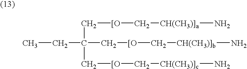
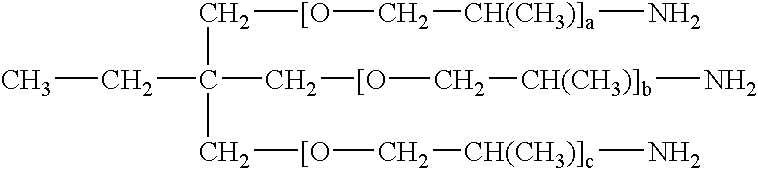
[0087] Surfactant: 2

[0088] (where a, b, and c are 20.)

[0089] Brightener: Na--SO.sub.3--(CH.sub.2).sub.3--S--S--(CH.sub.2).sub.3---SO.sub.3--Na

[0090] Current Density: 2 A / dm.sup.2

[0091] Plating Time: 60 minutes

[0092] Cathode: Build-Up Board

[0093] Cathode Area: 1 dm.sup.2

[0094] Anode: Titanium-Clad Platinum

[0095] Anode Area: 1 dm.sup.2

example 3

[0106] Copper Electroplating with Insoluble Anode Conditions for Copper Electroplating Plating Solution:

5 Sulfuric Acid 200 g / L Copper Sulfate 100 g / L Chloride Ion 60 mg / L Surfactant 0.50 g / L Brightener 5 mg / L

[0107] Surfactant: HO--(CH.sub.2--CH.sub.2--O).sub.120--H

[0108] Brightener: Na--SO.sub.3--(CH.sub.2).sub.3--O--CH.sub.2--S--CH.sub.-2--O--(CH.sub.2).sub.3--SO.sub.3--Na

[0109] Current Density: 2 A / dm.sup.2

[0110] Plating Time: 60 minutes

[0111] Cathode: Build-Up Board

[0112] Cathode Area: 1 dm.sup.2

[0113] Anode: Iridium Oxide

[0114] Anode Area: 1 dm.sup.2


PUM

PropertyMeasurementUnit
concentrationaaaaaaaaaa
depthaaaaaaaaaa
diameteraaaaaaaaaa

Abstract

The present invention provides a copper electroplating method using an insoluble anode, including: using an insoluble anode and a copper electroplating solution which contains a compound having a -X-S-Y- structure (where X and Y are each independently selected from the group consisting of a hydrogen atom, a carbon atom, a sulfur atom, a nitrogen atom, and an oxygen atom, and X and Y can be the same only where they are carbon atoms); and using direct current to plate a substrate. By this method, even a certain time period after the initial make-up of the electrolytic bath, stable deposition of the plated metal and formation of a filled via can be achieved, and an MVH can be filled up with the metal with no void left.

Description

[0001] The present invention relates to a copper electroplating method in which an insoluble anode and a copper electroplating solution that contains a specific compound having a sulfur atom are used, and a substrate is plated by using direct current. The present invention also relates to a composite material manufactured by the copper electroplating method.[0002] In recent years, with the advent of high performance and compact electronics such as personal computers, there has been a strong demand for printed wiring boards with higher density and reduced thickness. One of the methods to meet such a requirement uses a multilayered printed wiring board (build-up printed wiring board), which is manufactured through a build-up process including the steps of sequentially stacking layers and patterning the layers.[0003] Generally, such a build-up printed wiring board has a hole called a microvia hole (MVH) for electrical connection between adjacent layers, and the MVH is about 100 .mu.m i...

Claims


Application Information

Patent Timeline
Patent Type & Authority Applications(United States)
IPC IPC(8): C25D3/38
CPCC25D3/38Y10T428/8305
Inventor SEITA, MASARUTSUCHIDA, HIDEKIKUSAKA, MASARU
Owner SHIPLEY CO LLC
Why Eureka
Try Eureka