Plasma display device and method of producing the same

a technology of plasma and display device, which is applied in the manufacture of electrode systems, instruments, electric discharge tubes/lamps, etc., can solve the problems of lowering luminance, fluctuation of discharge start voltage or luminance, and difficulty in reliability, so as to improve reliability and life, lowering luminance, and lowering luminance

Inactive Publication Date: 2004-05-20
SONY CORP
View PDF1 Cites 13 Cited by
  • Summary
  • Abstract
  • Description
  • Claims
  • Application Information

AI Technical Summary

Benefits of technology

0009] The present inventors, as a result of their earnest studies for attaining the above object, have found out that when the trap density and/or the movable metallic ion density in the dielectric layer is set to be not more than a predetermined value; the fluctuation of discharge start voltage (driving voltage fluctuation) and the lowering of luminance would not easily be generated, and the reliability and life are enhanced. Based on the finding, the present invention has been completed. It is considered that the fluctuation of discharge start voltage (driving voltage fluctuation) and the lowering of luminance would n

Problems solved by technology

However, in the AC type plasma display device with the dielectric layer formed by the paste printing method, there is the problem of deterioration of the protective film.
Therefore, in the AC type plasma display device in which a thin dielectric layer composed

Method used


Image

  • Plasma display device and method of producing the same
  • Plasma display device and method of producing the same
  • Plasma display device and method of producing the same

Examples


first embodiment

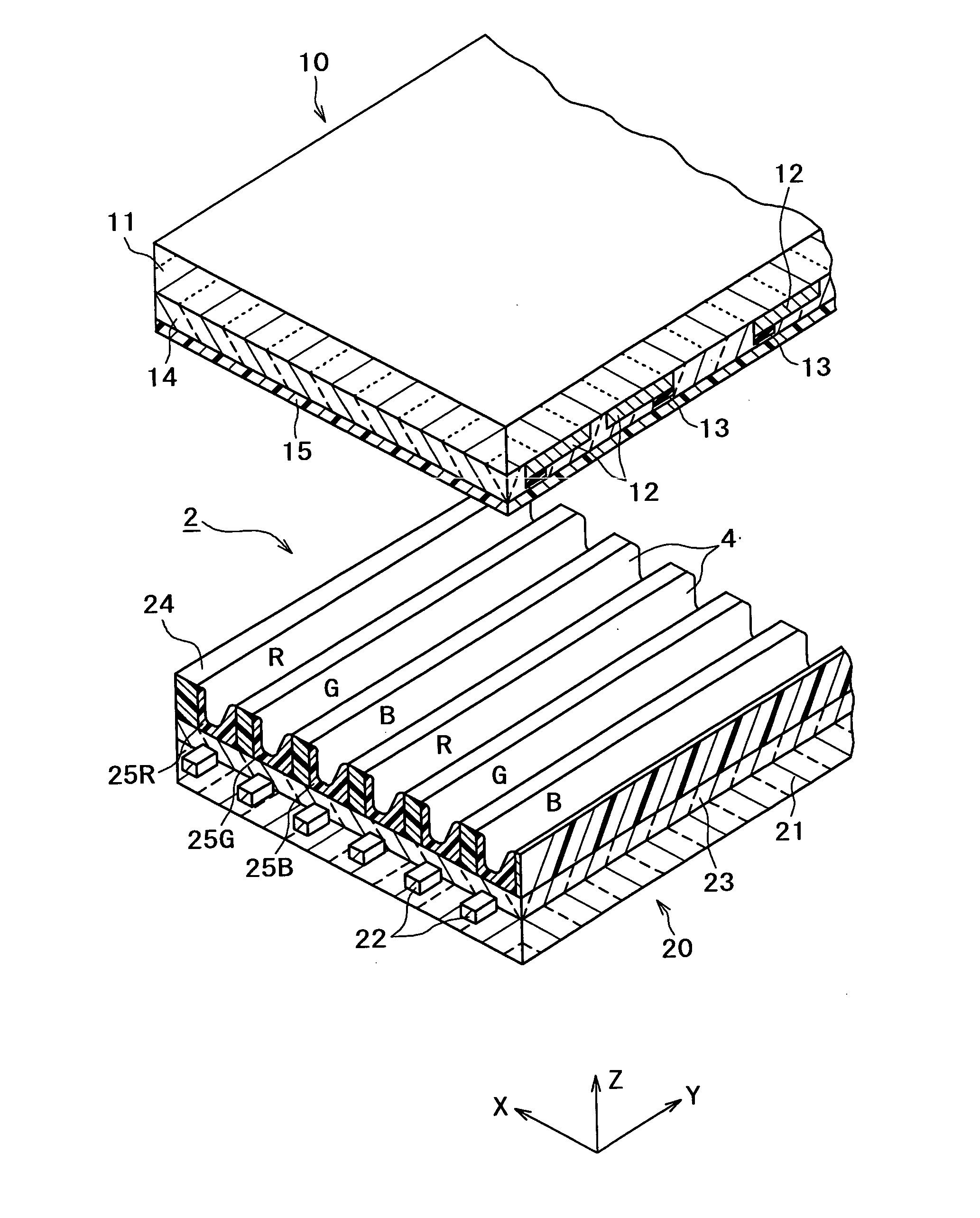
[0042] General Constitution of Plasma Display Device First, based on FIG. 1, the general constitution of an alternating current type (AC type) plasma display device (hereinafter sometimes referred to simply as a plasma display device) will be described.

[0043] An AC type plasma display device 2 shown in FIG. 1 belongs to the so-called three-electrode type, and electric discharge occurs between a pair of discharge sustaining electrodes 12. The AC type plasma display device 2 comprises a first panel 10 corresponding to a front panel, and a second panel 20 corresponding to a rear panel, which are laminated on each other. Light emission of phosphor layers 25R, 25G, 25B on the second panel 20 is observed, for example, through the first panel 10. Namely, the first panel 10 is on the display surface side.

[0044] The first panel 10 is comprised of a transparent first substrate 11, a plurality of pairs of discharge sustaining electrodes 12 provided in a stripe form on the first substrate 11 an...

second embodiment

[0080] In the above-described embodiment, the dielectric layer 14 composes of a single silicon oxide layer is formed by a sputtering method. However, in the present invention, the material properties of the layer and the film forming method therefor are not limited, as far as a dielectric layer having the trap density of not more than 1.times.10.sup.17 pieces / cm.sup.3 can be formed. In addition, in the present invention, the dielectric layer 14 may not necessarily be composes of a single silicon oxide layer, and may be composed of a multi-layer film.

third embodiment

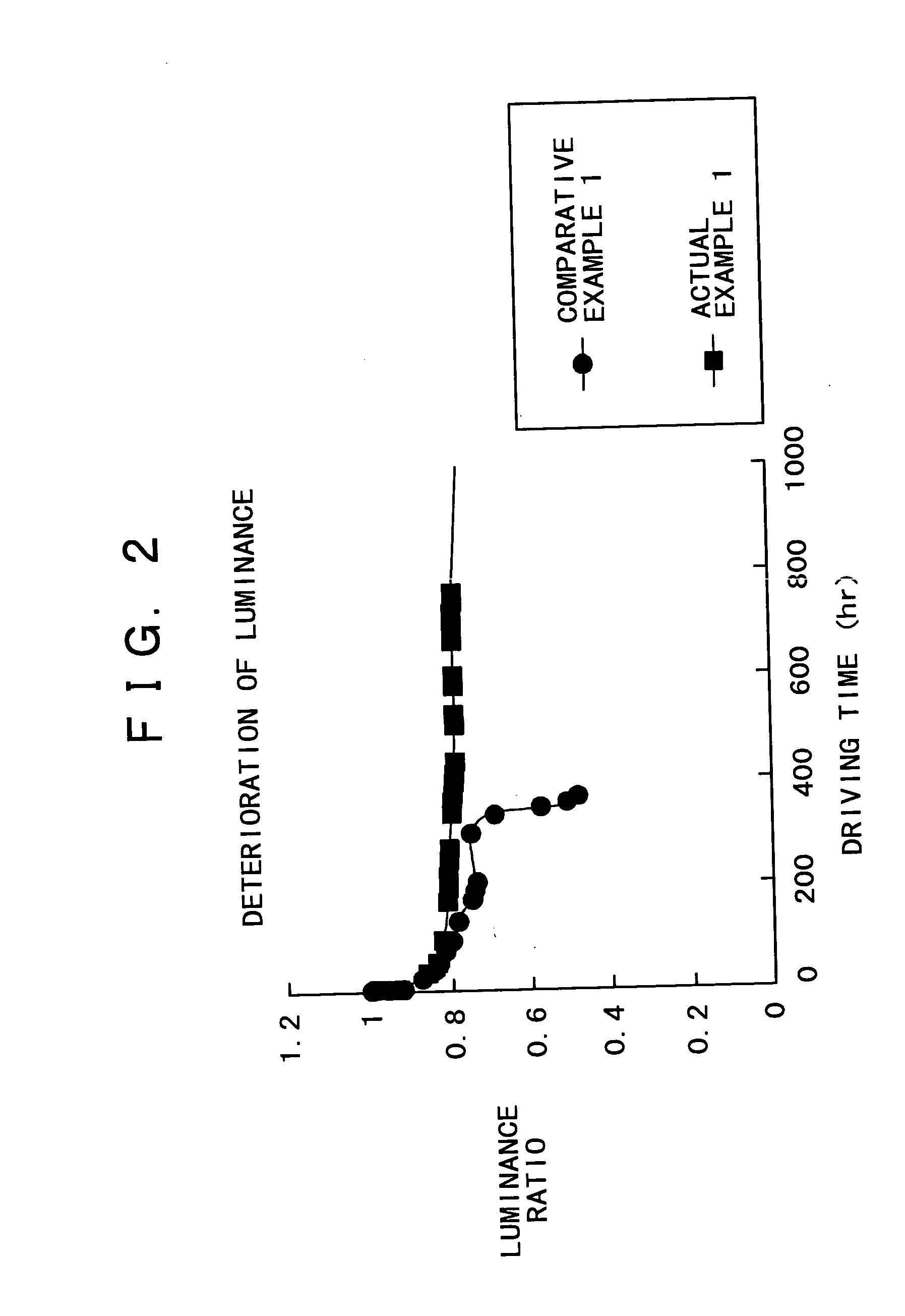
[0081] In the present embodiment, in the plasma display device 2 shown in FIG. 1, the relationship between the trap density in the dielectric layer 14 and the fluctuation of discharge start voltage will be described in more detail.

[0082] Generally, a large number of defects are present in a dielectric layer. It is well known that, in a glass containing silicon dioxide as a main constituent, the kind of the defects on an electric basis is the electron trap, in analogy to the thermal oxide SiO.sub.2 used for a MOS semiconductor. In the plasma display device, alkali metal- and alkaline earth-containing glasses containing silicon dioxide as a main constituent are in some cases used as an insulating material, on the discharge sustaining electrodes. In these glasses, components for controlling the melting point and dielectric constant, such as PbO, are also contained.

[0083] However, the discharge start voltage and the deterioration characteristics of the plasma display device differ great...


PUM


Abstract

A plasma display device such that fluctuation of discharge start voltage and lowering of luminance would not easily occur, the burning phenomenon of the screen is suppressed, and excellent reliability and long life can be secured, and a method of producing the same, are disclosed. The plasma display device comprises a first panel (10) provided with discharge sustaining electrodes (12) and a dielectric layer (14) on the inside thereof, and a second panel (20) laminated on the first panel (10) so that discharge spaces (4) are formed on the inside of the first panel (10), and the trap density and/or the movable metallic ion density in the dielectric layer (14) is not more than 1x10<18 >pieces/cm<3>, preferably not more than 1x10<17 >pieces/cm<3>.

Description

[0001] The present invention relates to a plasma display device and a method of producing the same. More particularly, the present invention relates to a plasma display device having characteristic features as to the trap density and / or the movable metallic ion density of a dielectric film formed on sustaining electrodes or as to the trap density and / or the movable metallic ion density of a dielectric film formed on address electrodes, and a method of producing the same.[0002] As a picture display device to be used in place of the cathode ray tube (CRT) which constitutes the main stream at present, a variety of flat panel type display devices have been investigated. Examples of such a flat panel type display device include liquid crystal display devices (LCD), electroluminescence display devices (ELD), and plasma display devices (PDP: plasma display panels). Among others, the plasma display devices have such merits as comparative easiness of an increase in screen size and an increas...

Claims


Application Information

Patent Timeline
IPC IPC(8): H01J9/02H01J11/12H01J11/22H01J11/24H01J11/26H01J11/34H01J11/38H01J17/49
CPCH01J9/02H01J11/38H01J11/12
Inventor KOJIMA, SHIGERUSUZUKI, TOSHIHARUSHIRAI, KATSUYA
Owner SONY CORP
Why Eureka
Try Eureka