

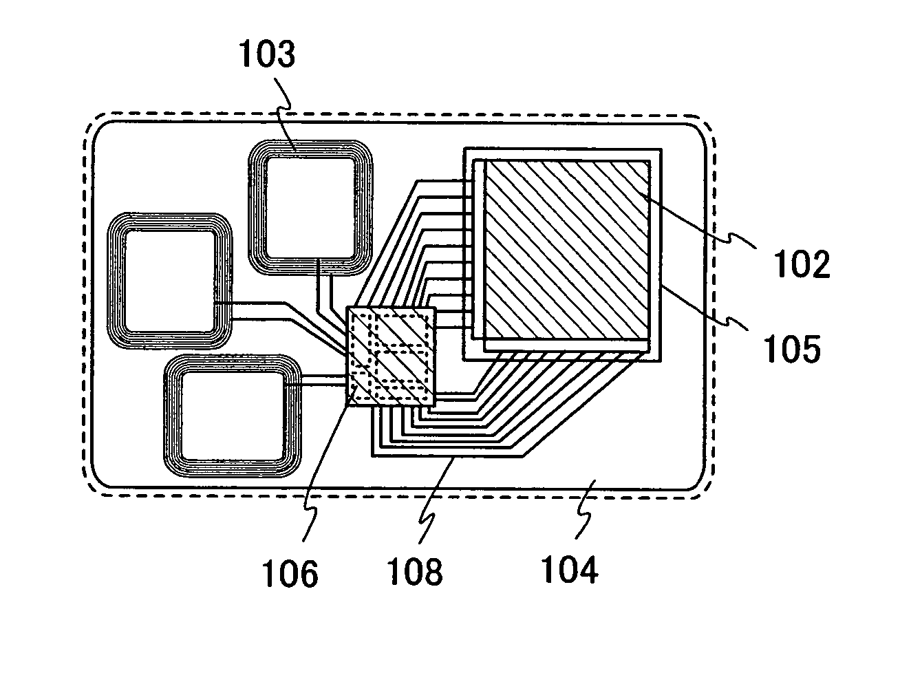
IC card and booking account system using the IC card
a technology of ic card and booking account, applied in the field of cards, can solve the problems of easy forgery, crack or grinding mark, and easy change of face picture by forgery,
- Summary
- Abstract
- Description
- Claims
- Application Information
AI Technical Summary
Benefits of technology
Problems solved by technology
Method used
Image

Examples
embodiment 1
[0144] In this embodiment, a liquid crystal material used when a first substrate is peeled-off after a liquid crystal display device is completed is described.
[0145] FIGS. 11A and 11B are cross sectional views of a liquid crystal display of this embodiment. A columnar spacer 1401 is provided with a pixel in a liquid crystal display device shown in FIG. 11A. Adhesion between a counter substrate 1402 and a substrate 1403 on the side of elements is enhanced by the columnar spacer 1401. This makes it possible to prevent a semiconductor element in the outside of the area overlapping with a sealing material from remaining on the side of the first substrate, when the first substrate is peeled off.
[0146] FIG. 11B is a cross sectional view of a liquid crystal display device using nematic liquid crystal, smectic liquid crystal, ferroelectric liquid crystal, or PDLC (polymer dispersed liquid crystal) in which the above described liquid crystal is included in polymer resin. Adhesion between the...
embodiment 2
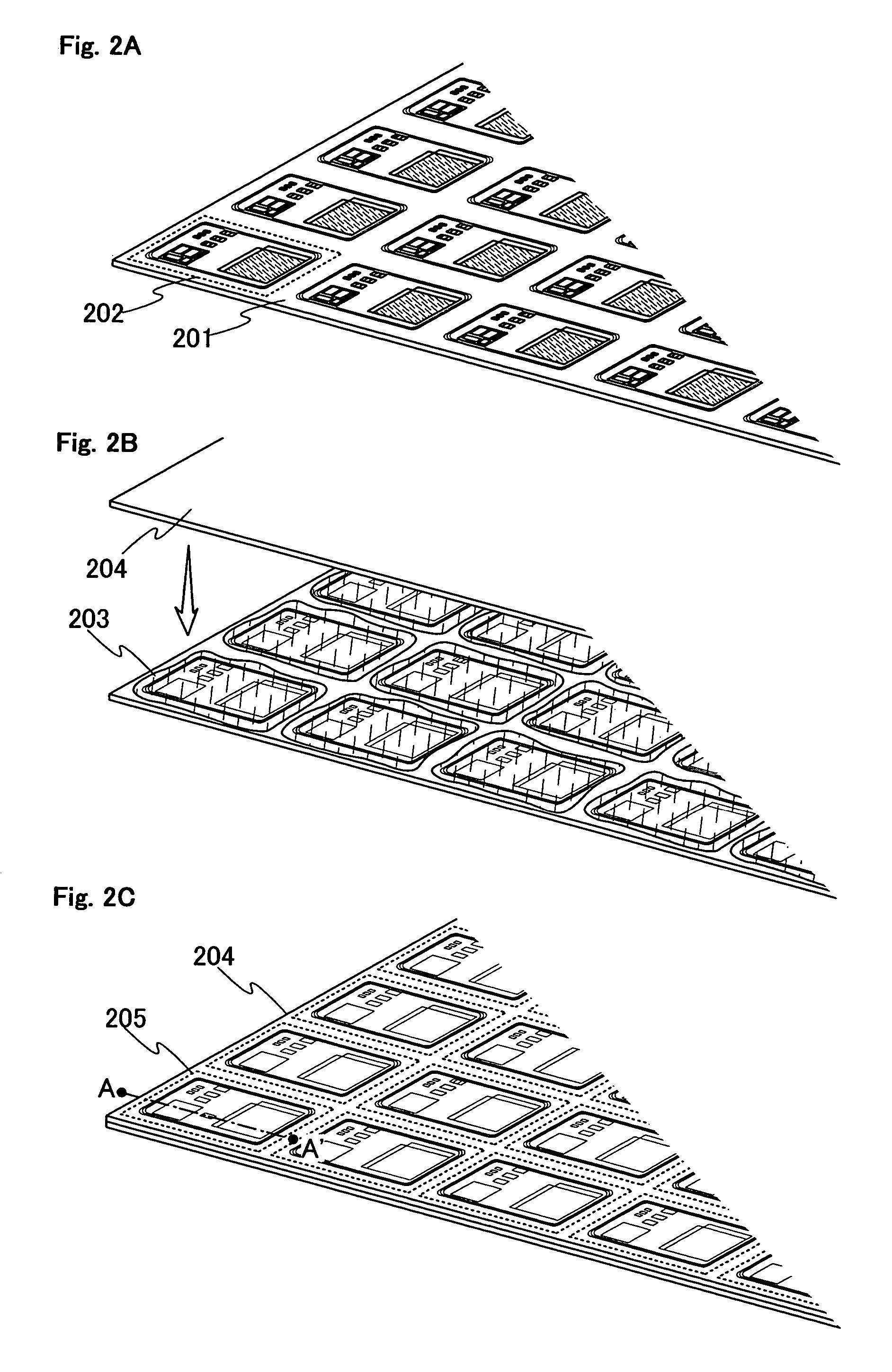
[0147] In this embodiment, a structure of a light-emitting device provided with the IC card in the present invention is described.
[0148] In FIG. 12, a base film 6001 is formed over a card substrate 6000. A transistor 6002 is formed over the base film 6001. The transistor 6002 is covered with a first interlayer insulating film 6006. A second interlayer insulating film 6007 and a third interlayer insulating film 6008 are laminated over the first interlayer insulating film 6006.
[0149] The first interlayer insulating film 6006 is formed by depositing a silicon oxide film, a silicon nitride film, or a silicon oxynitride film in a single layer or a laminate by plasma CVD or sputtering. A silicon oxynitride film in which mole fraction of oxygen is higher than that of nitrogen is laminated over a silicon nitride oxide film in which mole fraction of nitrogen is higher than that of oxygen to form a film. The film may be used as the first interlayer insulating film 6006.
[0150] A heat treatment...
embodiment 3
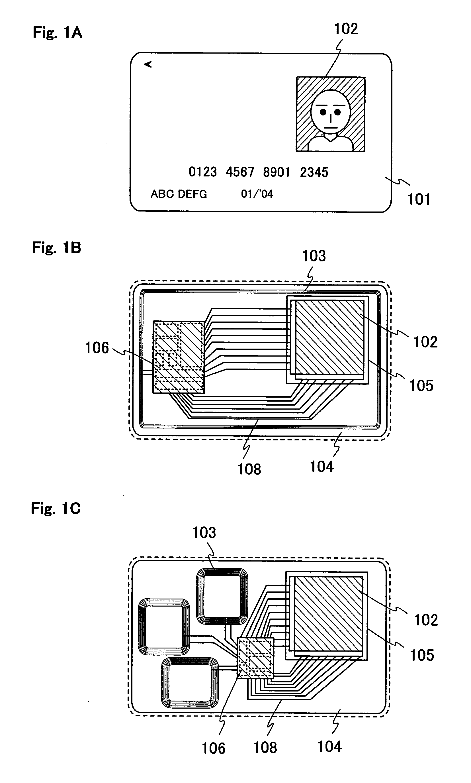
[0161] In this embodiment, a specific example of using an IC card of the present invention as an ATM card is described.
[0162] As shown in FIG. 13, image data of a bank depositor's face is memorized in a ROM provided with a thin film integrated circuit of an ATM card when the bank depositor opens an account in a financial institution such as a bank. Forgery such as changing the photograph of a human face can be prevented by memorizing the data thereof in the ROM. The ATM card is given to the bank depositor, and then he / she can begin to use the ATM card.
[0163] An ATM card is used for dealings at an ATM (automated teller machine) or a window. When dealing such as drawing, depositing, or transferring cash is done, details such as bank balance or dealing date is to be memorized in an EEPROM provided with a thin film integrated circuit of an ATM card.
[0164] After the dealing, details such as bank balance or dealing date may be displayed in a pixel portion of the ATM card, and the display ...
PUM
 Abstract
Description
Claims
Application Information