Printed wiring board and its manufacturing method

a printing method and manufacturing method technology, applied in metal-working apparatuses, solid-state devices, metallic material coating processes, etc., can solve the problems of poor ductility of thick plated copper layer formed by electroless plating, low elongation and high tensile strength characteristics, and tendency to develop cracks and other flaws

Active Publication Date: 2004-07-15
IBIDEN CO LTD
View PDF37 Cites 157 Cited by
  • Summary
  • Abstract
  • Description
  • Claims
  • Application Information

AI Technical Summary

Problems solved by technology

Moreover, the residual stress in the plated copper layer is fairly large so that the layer tends to develop cracks and other flaws and show low elongation and high tensile strength characteristics.
However, the thick plated copper layer formed by electroless plating is poor in ductility because of the unavoidable contamination of the layer with many impurities inclusive of the additives used.
Therefore, when a thick plated copper layer is formed by electroless plating, the reliability for the wiring and connection is insufficient and in order to attain a sufficient degree of reliability, an annealing step is indispensable in this case, too.
However, when the plated copper layer is formed by PC process, the uniformity of layer thickness is superior to that obtainable by direct current plating process but is not as good as the objective level (FIG. 4).
On the other hand, the plated copper layer formed by PR process is improved in the uniformity of thickness as compared with the layer obtainable by PC process but is not as high as desired yet and, moreover, plating by PR process requires an expensive current source.
However, with a plating solution containing EDTA as a complexing agent, a compressive stress (an expanding force) is generated in the plating metal layer to cause peeling of the plated copper film from the resin insulating layer.
Furthermore, there is also found the problem not to deposit within fine via holes not over 80 .mu.m in diameter.
Moreover, in the conventional processes for manufacture of printed circuit boards, it was impossible to construct fine-definition line conductor ...

Method used


Image

  • Printed wiring board and its manufacturing method
  • Printed wiring board and its manufacturing method
  • Printed wiring board and its manufacturing method

Examples


example 1

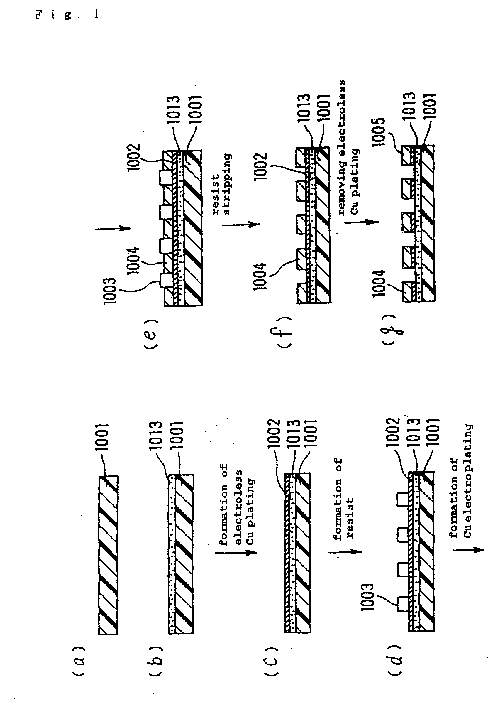
[0488] FIGS. 1 (a) to (g) show an exemplary process for fabricating the conductor circuit of the printed circuit board according to the invention and FIG. 2 (a) to (e) show an exemplary process for manufacturing a multilayer printed circuit board in accordance with the invention.

[0489] In constructing the conductor circuit on a printed circuit board, an insulating substrate 1001 of glass cloth-epoxy resin or BT material was used as the insulating sheet as shown in FIG. 1 (a).

[0490] Then, 35 weight parts of acrylate (25 wt. %) of cresol novolac epoxy resin (Nippon Kayaku; mol. wt. 2500), 3.15 weight parts of photosensitive monomer (Toa Gosei Co.; trade mark, Aronix M315), 0.5 weight part of antifoam (Sun Nopco, S-65), 3.6 weight parts of N-methylpyrrolidone (NMP), 12 weight parts of polyethersulfone (PES), and epoxy resin powders (Sanyo Kasei; Polymerpol; 1.0 .mu.m of average particle diameter, 7.2 wt. Parts, and 0.5 .mu.m of average particle diameter, 3.09 wt. parts) were mixed toge...

example 2

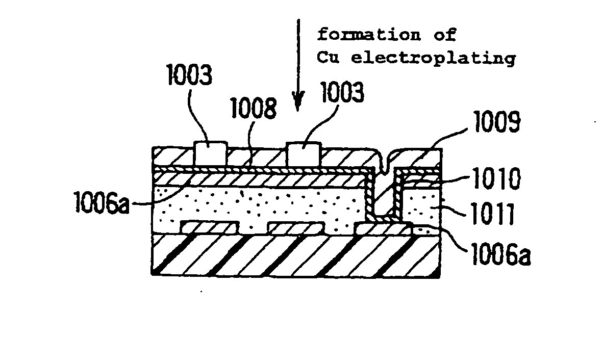
[0524] The following is an example of application of this invention to the manufacture of a CMOS IC chip.

[0525] An IC wafer was fabricated by the well-known MOS wafer production technology, for example by the process described in LSI Process Engineering, pp. 22 to 23 (Published by Ohm-sha, K.K., Jun. 20, 1987] [FIG. 10 [a)].

[0526] The whole surface of a substrate was subjected to Cu sputtering to provide a Cu layer 1014 in a thickness of 0.6 .mu.m (FIG. 10 (b)). Cu sputtering can be carried out using a vacuum sputtering equipment (Tokuda Seisakusho; CFS-8EP).

[0527] Then, using a spin coater, a negative photoresist (Tokyo Auka Kogyo; OMR83) was coated on the Cu layer 1014, followed by drying. Thereafter, prebaking, exposure, development and postbaking were performed in succession to provide a plating resist 1015 (4 .mu.m thick, L / S=20 / 20 .mu.m). Then, the sheet was immersed in 10% aqueous solution of sulfuric acid for surface activation and constant-voltage pulse copper electroplatin...

example 3

[0529] A. Preparation of a Resin Composition for Forming Roughened Surface

[0530] Mixing 34 weight parts of the resin solution dissolving 25% acrylate of a cresol novolac epoxy resin (Nippon Kayaku, mol. wt. 2500 ) in diethylene glycol dimethyl ether (DMDG), and, 2 weight parts of imidazole curing agent (Shikoku Kasei; 2E4MZ-CN), 4 weight parts of the photosensitive monomer caprolactone-modified tris (acryloxylethyl) isocyanurate (Toa Gosei; trade mark, Aronix M325), 2 weight parts of the photopolymerization initiator benzophenone (Kanto Chemical), 0.2 weight part of the photosensitizer Michler's ketone (Kanto Chemical), 10 weight parts of photosensitive monomer (Nippon Kayaku; KAYAMER PM-21), and epoxy resin powders (Sanyo Kasei, trade mark, Polymerpole; average particle diameter 1.0 .mu.m, 15 weight parts and average particle diameter 0.5 .mu.m, 10 weight parts), and with addition of 30.0 weight parts of N-methylpyrrolidone (NMP), the mixture was adjusted to a viscosity of 7 Pa.cnd...


PUM

PropertyMeasurementUnit
Fractionaaaaaaaaaa
Timeaaaaaaaaaa
Linear densityaaaaaaaaaa

Abstract

The present invention has for its object to provide a process for manufacturing multilayer printed circuit boards which is capable of simultaneous via hole filling and formation of conductor circuit and via holes of good crystallinity and uniform deposition can be constructed on a substrate and high-density wiring and highly reliable conductor connections can be realized without annealing. The present invention is related to a process for manufacturing multilayer printed circuit boards which comprises disposing an interlayer resin insulating layer on a substrate formed with a conductor circuit, creating openings for formation of via holes in said interlayer resin insulating layer, forming an electroless plated metal layer on said interlayer resin insulating layer, disposing a resist thereon, performing electroplating, stripping the resist off and etching the electroless plated metal layer to provide a conductor circuit and via holes, wherein the electroplating is performed intermittently using said electroless plated metal layer as cathode and a plating metal as anode at a constant voltage between said anode and said cathode.

Description

[0001] The present invention relates to a printed circuit board and to a method for production thereof. The invention further relates to plating methods and plating solutions which can be applied to the above production of printed circuit boards. BACKGROUND ART[0002] With the mounting need for higher functionality and further miniaturization of electronic equipment, advances in integration technology of LSI and in size reduction of components, and changes in the mounting mode, the demand for high-density wiring is getting greater in the field of printed circuit boards and, as a consequence, development of the so-called multilayer circuit boards comprising 3 or more conductor layers has been broadly undertaken.[0003] In view of the demand for higher wiring density in multilayer circuit boards, the so-called buildup multilayer circuit board is attracting attention. The buildup multilayer circuit board is manufactured by the technology disclosed in Japanese Kokai Publication Hei-4-5555...

Claims


Application Information

Patent Timeline
IPC IPC(8): C23C18/34C25D5/18H05K3/00H05K3/10H05K3/18H05K3/24H05K3/38H05K3/42H05K3/46
CPCC23C18/1607Y10T29/49155C23C18/22C23C18/30C23C18/34C23C18/405C23C28/023C25D3/38C25D5/022C25D5/18C25D5/34H05K3/0038H05K3/108H05K3/181H05K3/241H05K3/381H05K3/382H05K3/384H05K3/421H05K3/423H05K3/427H05K3/4602H05K3/4644H05K3/4652H05K3/4661H05K2201/0215H05K2201/0344H05K2201/0347H05K2201/09509H05K2201/09536H05K2201/09563H05K2201/0959H05K2201/096H05K2203/0353H05K2203/0723H05K2203/1476H05K2203/1492C23C28/42C23C28/00C25D7/123Y10T29/49126Y10T29/49156Y10T29/49165Y10T29/49128C23C18/1653H01L2224/16225H01L2924/15174H01L2924/15311C25D5/625C25D5/617C23C18/54
Inventor EN, HONCHINNAKAI, TOHRUOKI, TAKEOHIROSE, NAOHIRONODA, KOUTA
Owner IBIDEN CO LTD
Why Eureka
Try Eureka