

Method, structure, and apparatus for Raman spectroscopy
a raman spectroscopy and apparatus technology, applied in the field of raman spectroscopy, can solve the problems of limiting the practicality of conventional raman spectroscopy apparatus, needing powerful and costly laser sources for excitation and other prohibitively expensive equipment, and undesired background fluorescen
- Summary
- Abstract
- Description
- Claims
- Application Information
AI Technical Summary
Problems solved by technology
Method used
Image

Examples
example 1
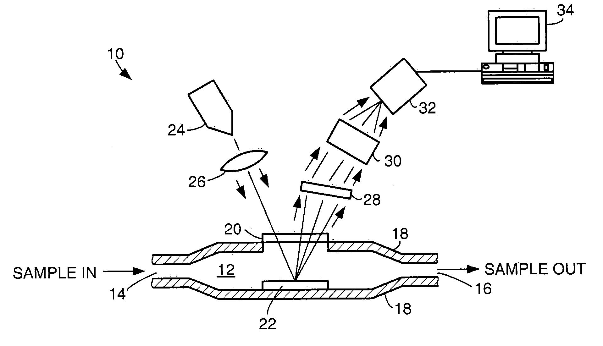
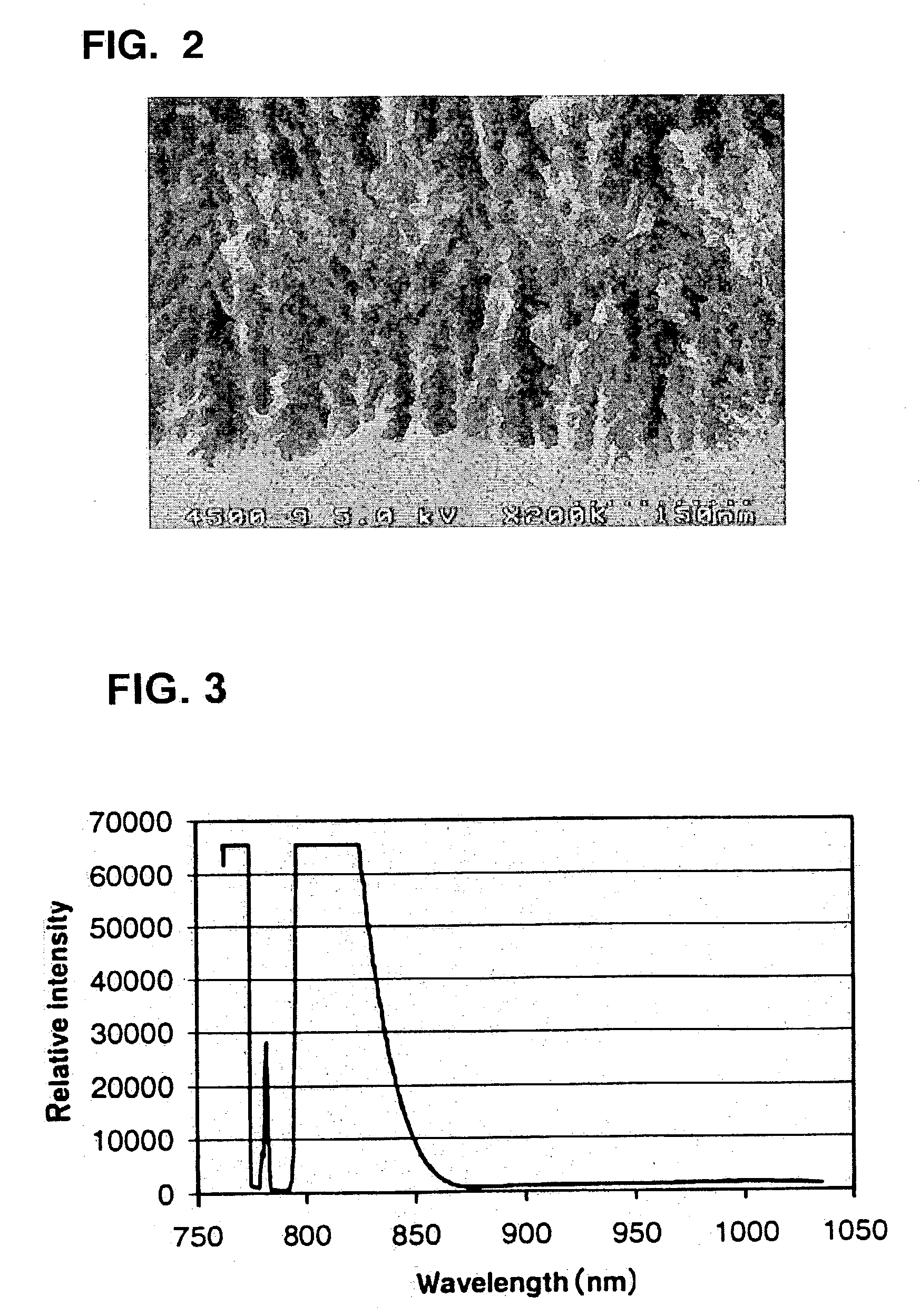
[0038] Shown in FIG. 2 is a scanning electron microscope (SEM) micrograph image of a porous silicon substrate for use with the Raman spectroscopy apparatus. The substrate was prepared by anodic, electrochemical etching, as described above. More specifically, the substrate was prepared by subjecting a highly boron-doped, p-type silicon wafer to etching in an aqueous electrolyte solution containing ethanol and HF present in a concentration of about 15 percent by volume based on the total volume of the solution (15% HF by volume). Anodization was carried out by a computer-controlled constant current applied across the cell (between a platinum cathode and the silicon anode). Multiple layers of porous silicon were produced from 5 periods of two different current density settings. One such setting was at 5 mA / cm.sup.2 for 20 seconds, which provided a layer having a porosity of about 42% and a thickness of about 80 nm. The other setting was at 30 mA / cm.sup.2 for 10 seconds, which provided ...
PUM
| Property | Measurement | Unit |
|---|---|---|
| porosity | aaaaa | aaaaa |
| refractive index | aaaaa | aaaaa |
| thickness | aaaaa | aaaaa |
Abstract
Description
Claims
Application Information