Although some conventional efforts have been directed to increase the amount of light extraction by effectively spreading the current throughout the device through improving shape of the electrode, increase in the electrode area is inevitable in anyway, and this causes a dilemma that the amount of light extraction is restricted instead by decrease in the narrowing of the light extraction area.
This undesirably results in concentration of
current density to the electrode-covered region, and reduction in the substantial amount of light extraction from the light extraction region.
Bonding of the electrode wire to the bonding pad is, however, disadvantageous in that damages ascribable to the bonding are likely to adversely affect the light emitting layer portion, and are likely to cause failures.
The thus-configured, current-spreading layer need to be raised in the
dopant concentration in order to ensure the conductivity, and this tends to result in the problems below.
This undesirably reduces probability of radiative recombination, and consequently lower the
emission intensity.
That is, time-dependent degradation of the emission luminance becomes more likely to degrade, so that the device lifetime also tends to degrade.
The current-spreading layer, tried to be grown by the MOVPE process or the LPE process, raises another problem in that high growth temperatures in these processes make the
dopant more likely to diffuse towards the cladding layer side intrinsically expected to have a low dopant concentration.
In addition, growth of a thick current-spreading layer needs a longer time and a larger amount of raw materials, and this tends to lower the production efficiency and to increase the cost.
Once this situation occurs, a photo
lithography process for forming electrodes or the like, or dicing of a
wafer for producing device chips, carried out on the device
wafer having the ITO electrode layer already formed thereon, is likely to cause exfoliation of the ITO electrode layer, and this directly results in lowering in
yield ratio of the product.
Our investigations into the back ground art same as those described in the first and second inventions revealed that the transparent conductive layer composed of ITO tends to raise the
contact resistance with the
compound semiconductor layer on the device side if used in an intact form, and inevitably lowers the
emission efficiency due to increased series resistance.
It is, however, unconditionally necessary, in view of securing a desirable
ohmic contact, to configure the
electrode contact layer using InGaAs or the like having a small
band gap energy, and this inevitably raises a problem that only a small thickness thereof inevitably result in lowered extraction efficiency due to light absorption.
Another problems resides in that, in a fabrication process of the device, a bonding pad to which a current supply wire is to be bonded must be formed anyway on the electrode even if the electrode is formed with a transparent material.
In this device, the drive
voltage tends to concentrate into the formation region of the bonding pad which is composed of a highly-conductive
metal, but tends to be scarce in the region surrounding the pad, which serves as the light extraction region, so that the light extraction efficiency becomes more likely to decrease, and an effect of adopting the transparent electrode cannot always be exhibited to a satisfactory degree.
(1) direct lowering of the emission luminance, which is supposed to be mainly ascribable to an increased contribution of the non-
radiative transition processes caused by the
crystal defect; and
(2) shortened lifetime of the device, which is ascribable to the damaged region possibly formed in the light emitting layer portion. If the light emitting layer portion having
dislocation formed therein is kept under a consecutive current supply, the current concentrates to the
dislocation and tends to proliferate it, and this results in a time-dependent degradation of the emission luminance.
The thickness exceeding 5 .mu.m will undesirably increase the resistivity in the thickness-wise direction due to its low dopant concentration, and will result in lowered
emission efficiency due to increased series resistance of the device.
The thick
cushion layer is also disadvantageous in that the growth thereof needs a longer time and a larger consumption of the source materials, and this tends to lower the production efficiency and to increase the cost.
For a specific case where the light emitting layer portion is composed of AlGaInP, and the second-conductivity-type cladding layer is configured as a p-type cladding layer containing Zn as a p-type dopant, it is undesirable to dispose the current-spreading layer having a large Zn concentration in contact therewith, because
back diffusion of Zn is very likely to proceed and the
emission efficiency tends to degrade.
The majority carrier concentration smaller than 5.times.10.sup.16 / cm.sup.3 will increase the series resistance of the device, and thus result in degradation of the emission efficiency.
The concentration equal to or exceeding 1.times.10.sup.18 / cm.sup.3 will make it more likely to cause defect levels which serve as a non-radiative recombination center, and this will again result in degradation of the emission efficiency.
The concentration exceeding 9.times.10.sup.17 / cm.sup.3 will make it more likely to accelerate
diffusion of the dopant atom from the
cushion layer to the light emitting layer portion side due to electrical factors, and this eventually degrades the device lifetime.
Although growth of a thick current-spreading layer as in the conventional device by the MOVPE process, characterized by a relatively
slow growth speed, results in a considerable decrease in the production efficiency, the cushion layer, which is desired to be formed with a small thickness as described in the above hardly causes the problem of decrease in the efficiency even when the MOVPE process is adopted.
Under a relatively large tendency of the dopant
diffusion from the
electrode contact layer to the cushion layer, an excessively larger amount of addition of the dopant in the electrode
contact layer over the cushion layer may result in electrical acceleration of the dopant
diffusion from the electrode
contact layer to the cushion layer during emission current supply, and this may gradually deplete the amount of dopant in the electrode
contact layer.
This undesirably increases the contact resistance of the electrode contact layer with the elapse of time of the current supply, and results in degradation of the device lifetime.
The electrode contact layer formed so as to cover the entire portion of the contact surface with the oxide transparent electrode layer lowers contact resistance of the oxide transparent electrode layer also in the region right under the boding pad for
wire bonding, but this makes the drive current or
light emission more likely to concentrate within that region, so that a large portion of the emitted light is intercepted by the bonding pad, and thereby the light extraction efficiency is degraded.
In the conventional light emitting device having a thick current-spreading layer formed therein in order to raise the current spreading effect, there has been adopted a
blocking layer having a conductivity type opposite to that of the current-spreading layer formed so as to be buried in the current-spreading layer, in order to bypass the current outside the region right under the bonding pad, but this was disadvantageous in that the device configuration becomes more complicated, and the number of process steps for the fabrication increases.
The oxide transparent electrode layer such as the ITO layer may sometimes fail in forming a desirable
ohmic contact in
direct bonding with the bonding-side compound
semiconductor layer, and may lower the emission efficiency due to increased series resistance based on the contact resistance.
(1) direct lowering of the emission luminance, which is supposed to be mainly ascribable to an increased contribution of the non-
radiative transition processes caused by the
crystal defect; and
(2) shortened lifetime of the device, which is ascribable to the
dislocation possibly formed in the light emitting layer portion. If the light emitting layer portion having dislocation formed therein is kept under a consecutive current supply, the current concentrates to the dislocation and tends to proliferate it, and this results in a time-dependent degradation of the emission luminance.
The thickness of the bonding-side
semiconductor layer of less than 0.6 .mu.m will make influences of the damage ascribable to the bonding more likely to extend to the active layer, and will cause degradation of the
emission intensity and device lifetime.
On the other hand, since the dopant concentration of the bonding-side semiconductor layer is suppressed to a relatively low level, the thickness thereof equals to or exceeding 10 .mu.m will undesirably result in excessive increase in the series resistance of the device.
The thickness exceeding 5 .mu.m will undesirably increase the resistivity in the thickness-wise direction due to its low dopant concentration, and will result in lowered emission efficiency due to increased series resistance of the device.
The thick cushion layer is also disadvantageous in that the growth thereof needs a longer time and a larger consumption of the source materials, and this tends to lower the production efficiency and to increase the cost.
The thickness exceeding 30 nm may undesirably result in
increased effect of the light absorption, and the thickness less than 3 nm may make it difficult to keep a
bulk crystal structure and to obtain a sufficient effect of reducing the contact resistance.
Any excessively elevated annealing temperature or excessively prolonged annealing time, however, undesirably promotes the In diffusion from the ITO layer, and this makes the In concentration profile in the electrode contact layer kept constant at a relatively high level as shown by curve {circle over (3)} in FIG. 15, where the above-described effects become not attainable.
The In concentration based on the above definition less than 0.1 may result in only an insufficient effect of reducing the contact resistance of the electrode contact layer, and exceeding 0.6 may considerably worsen the quality degradation such as lowered
emission intensity due to
lattice mismatch between the electrode contact layer and the light emitting layer portion.
The annealing temperature exceeding 750.degree. C. may result in an excessive
diffusion velocity of In into the GaAs layer, and this is highly causative of an excessive In concentration in the electrode contact layer.
This also results in saturation of the In concentration and makes it difficult to obtain the In concentration profile graded in the thickness-wise direction of the electrode contact layer.
The excessive In diffusion into the GaAs layer also drains In in the ITO electrode layer in the vicinity of the contact portion with the electrode contact layer, and inevitably raises electric resistance of the electrode.
In addition, too high annealing temperature exceeding 750.degree. C. allows
oxygen in ITO to diffuse towards the GaAs layer and oxidize it, and this tends to raise the series resistance of the device.
All of these are causative of nonconformities such that the light emitting device is not operable at an appropriate
voltage.
An extremely high annealing temperature may also impair the conductivity of the ITO electrode layer.
On the contrary, the annealing temperature less than 600.degree. C. may result in too small In
diffusion velocity into the GaAs layer and considerably lower the production efficiency, because a longer time will be necessary to obtain the electrode contact layer with sufficiently lowered contact resistance.
On the other hand, the annealing time shorter than 5 seconds may result in only an insufficient amount of In diffusion into the GaAs layer, and this makes it difficult to obtain the electrode contact layer with sufficiently lowered contact resistance.
In this case, the larger the amount of addition of the dopant to the electrode contact layer increases, the lower the contact resistance becomes.
Under a relatively large tendency of the dopant diffusion from the electrode contact layer to the bonding-side semiconductor layer, an excessively larger amount of addition of the dopant in the electrode contact layer over the bonding-side semiconductor layer may result in electrical acceleration of the dopant diffusion from the electrode contact layer to the bonding-side semiconductor layer during emission current supply, and this may gradually deplete the amount of dopant in the electrode contact layer.
This undesirably increases the contact resistance of the electrode contact layer with the elapse of time of the current supply, and results in degradation of the device lifetime.
In the conventional light emitting device having a thick current-spreading layer formed therein in order to raise the current spreading effect, there has been adopted a
blocking layer having a conductivity type opposite to that of the current-spreading layer formed so as to be buried in the current-spreading layer, in order to bypass the current outside the region right under the bonding pad, but this was disadvantageous in that the device configuration becomes more complicated, and the number of process steps for the fabrication increases.
In this case, the suppressive effect over the
phosphorus diffusion towards the ITO electrode layer can be achieved without problems, while the improving effect of the device lifetime remains not expectable.
As has been described in the above, the oxide transparent electrode layer such as the ITO layer cannot always be successful in forming a desirable ohmic contact when brought into direct contact with the semiconductor layer on the device side, and may cause degradation in the emission efficiency due to increase in the series resistance ascribable to the contact resistance.
The thickness exceeding 30 nm may undesirably result in
increased effect of the light absorption, and the thickness less than 3 nm may make it difficult to keep a
bulk crystal structure and to obtain a sufficient effect of reducing the contact resistance.
(1) direct lowering of the emission luminance, which is supposed to be mainly ascribable to an increased contribution of the non-
radiative transition processes caused by the
crystal defect; and
(2) shortened lifetime of the device. If the light emitting layer portion having dislocation formed therein is kept under a consecutive current supply, the current concentrates to the dislocation and tends to proliferate it, and this results in a time-dependent degradation of the emission luminance.
It is to be noted that the upper limit of the thickness is set to 10 .mu.m, because the bonding-side semiconductor layer formed with an excessively large thickness results in only a degraded production efficiency of the light emitting device.
The thickness of less than 0.1 .mu.m tends to result in only an insufficient
total thickness of the bonding-side semiconductor layer, so that the influence of the electrode
wire bonding becomes more likely to exert on the light emitting layer portion.
Whereas the thickness exceeding 5 .mu.m will undesirably increase the resistivity in the thickness-wise direction due to its low dopant concentration, and will result in lowered emission efficiency due to increased series resistance of the device.
The thick cushion layer is also disadvantageous in that the growth thereof needs a longer time and a larger consumption of the source materials, and this tends to lower the production efficiency and to increase the cost.
In this case, the suppressive effect over the
phosphorus diffusion towards the ITO electrode layer can be achieved without problems, while the improving effect of the device lifetime remains not expectable.
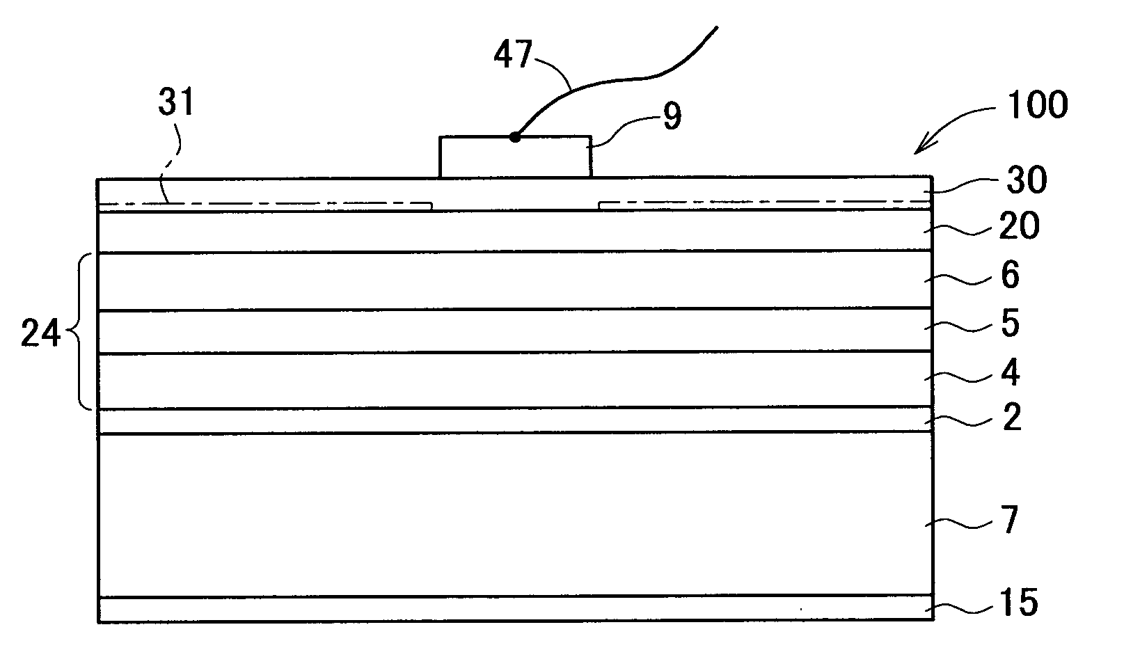
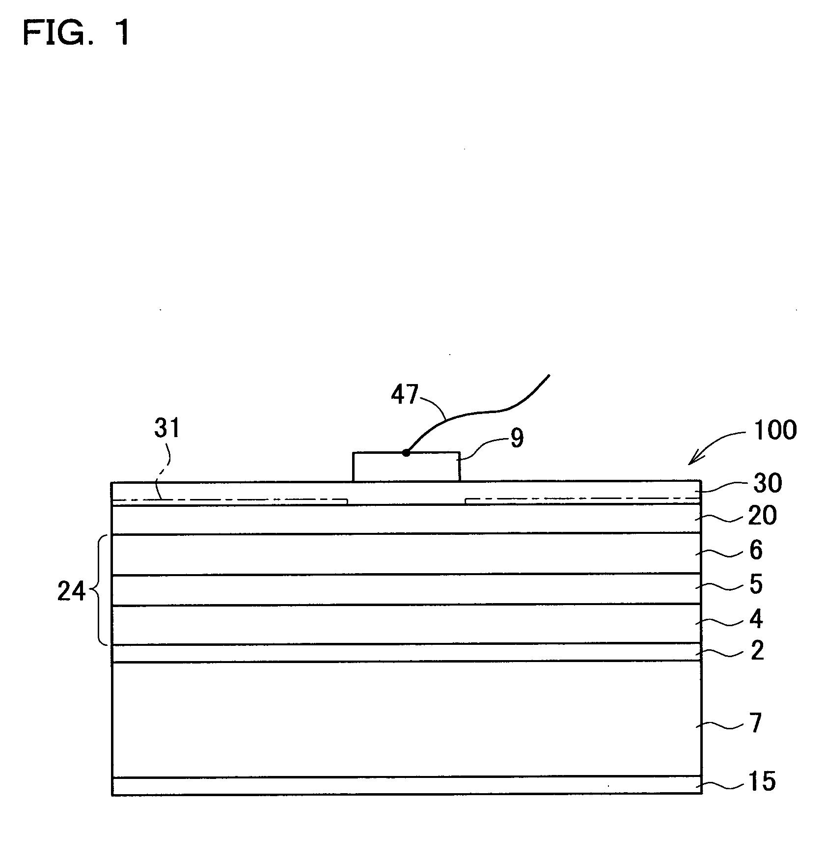
In an exemplary case where the light emitting layer portion 24 is formed right under the oxide transparent electrode layer 30 as shown in FIG. 5, the damaged region DM may extend to reach the light emitting layer portion 24, and this may result in failures in the characteristics such as degraded emission luminance or device lifetime.
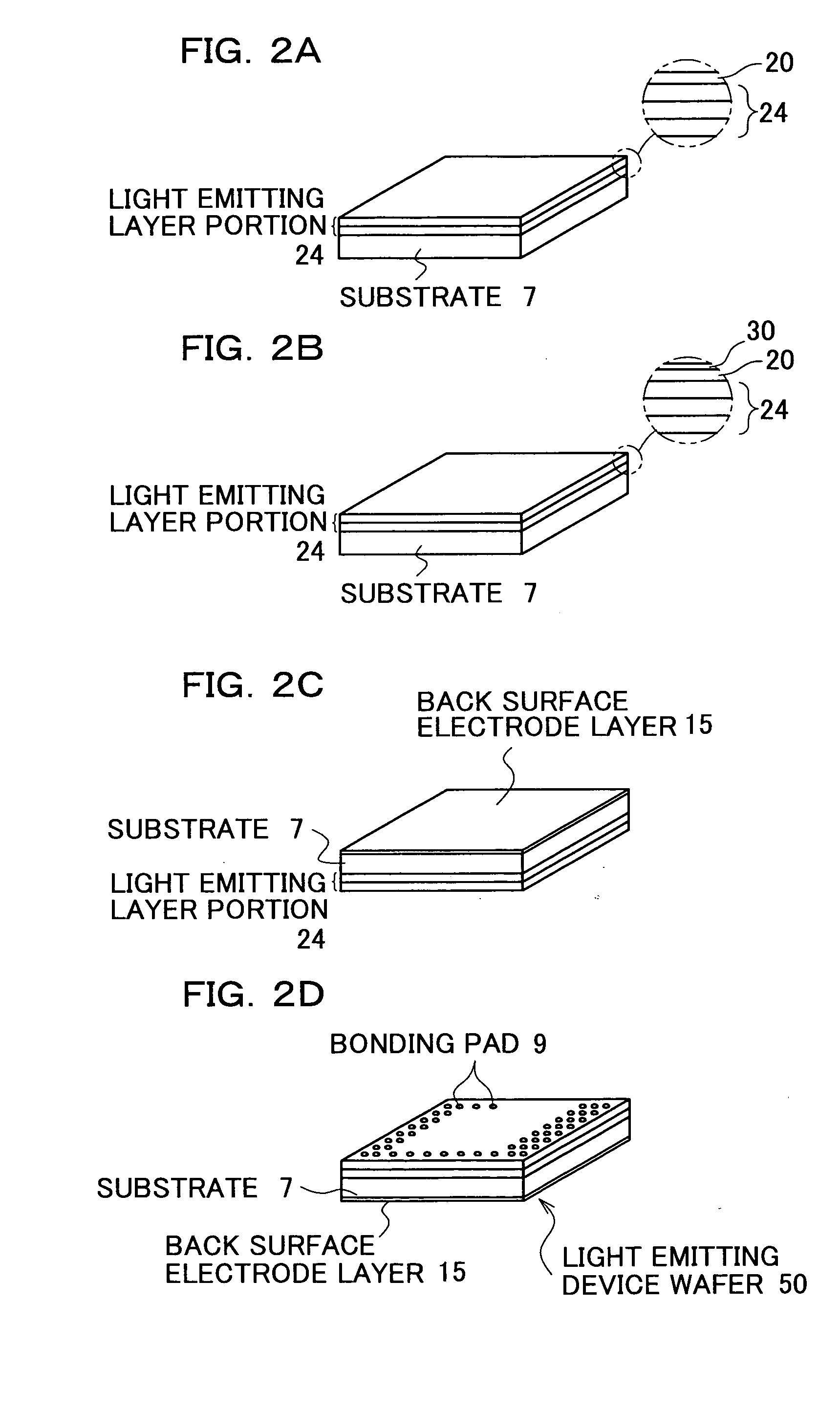
The ITO electrode layer 30 becomes more likely to exfoliate in particular during the patterning of the bonding pad 9 by
photolithography in the process step shown in FIG. 2D, during the half-dicing in the process step shown in FIG. 3A, and during the mesa-
etching in the process step shown in FIG. 3B, and this tends to result in failure or degradation in the production yield.

