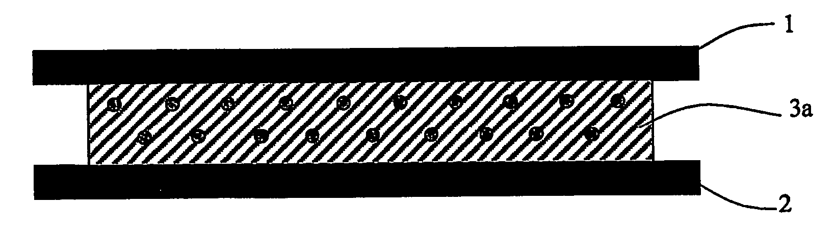
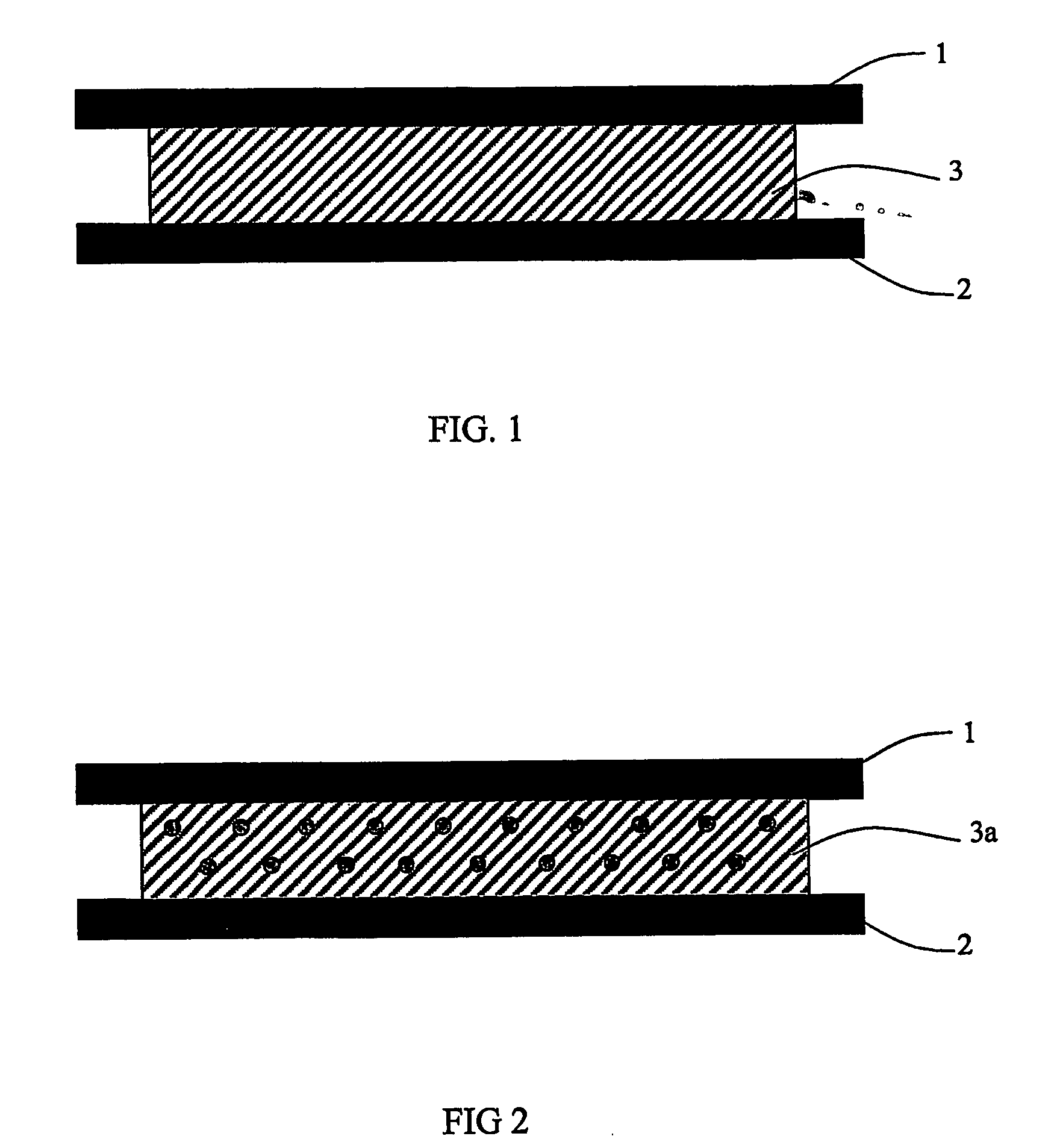
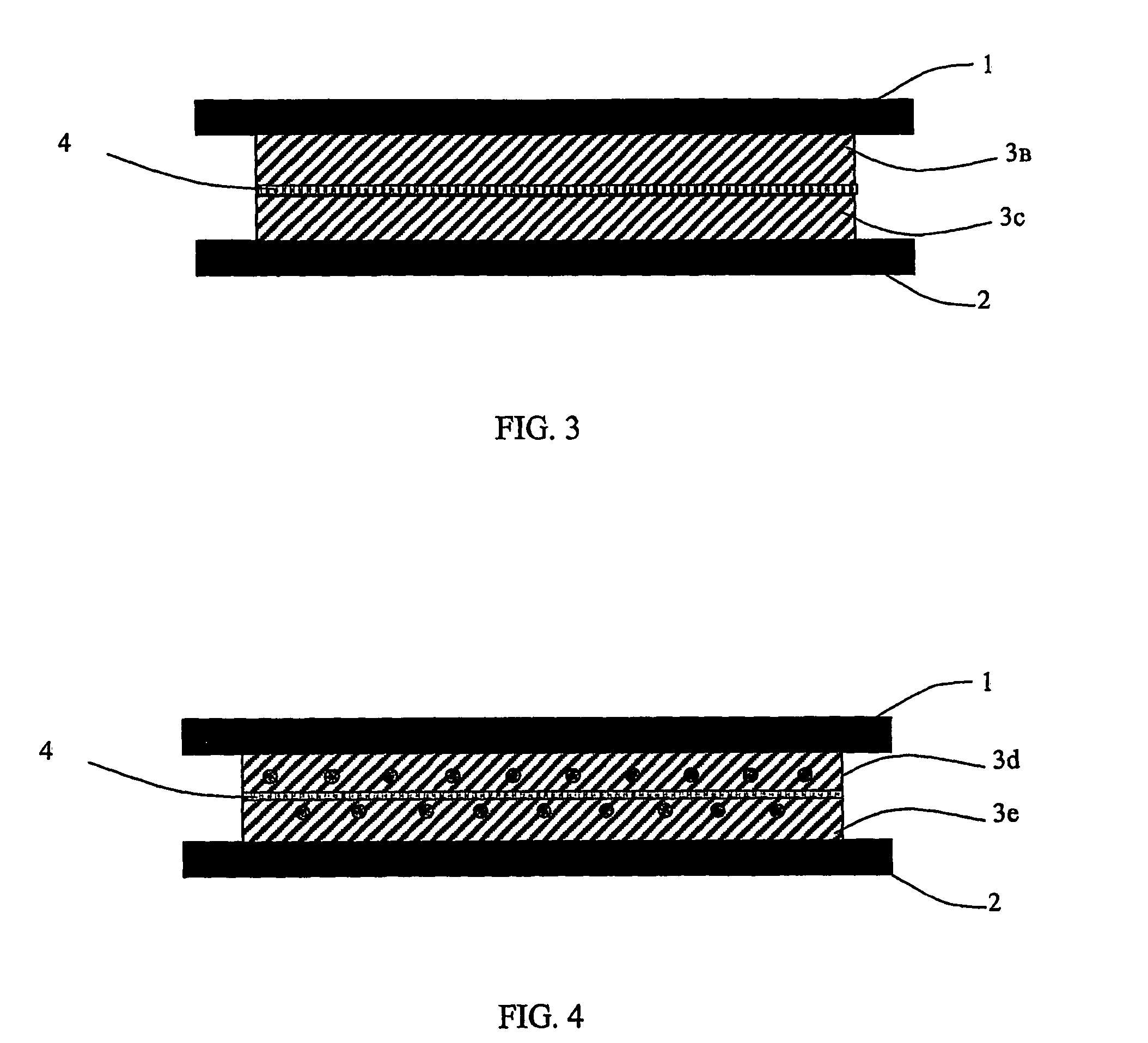
[0039] The claimed memory cell (FIGS. 1 through 8) contains two continuous aluminum electrodes 1 and 2 between which there is a single layer functional zone consisting of one active layer which can be doped by ions 3 or electrolyte clusters 3a (FIG. 1-2) or two active doped layers 3b and 3c (FIG. 3) or two active layers with electrolyte clusters 3d and 3e (FIG. 4) separated by a barrier layer 4. FIGS. 5 through 8 show the multilayer functional zones, consisting of one active layer 3 and one passive layer 5 (FIG. 5) or of one active layer 3, one barrier layer 4 and one passive layer 5 (FIG. 7) or of two active layers 3b and 3c, one barrier layer 4 and two passive layers 5a and 5b (FIG. 8).
[0040] In FIGS. 9 through 11 the claimed memory cell contains aluminum electrodes 1 and 2 where the top electrode 1 consists of two elements 1a and 1b. Between the electrodes there is a single layer functional zone, consisting of one active layer 3 (FIG. 9) or a multilayer functional zone consisting of one active layer 3 and one passive layer 5 (FIG. 10) or a multilayer functional zone consisting of one active layer 3, one barrier layer 4 and one passive layer 5 (FIG. 11).
[0041] FIGS. 12 through 14 show the claimed memory cell that has aluminum electrodes 1 and 2, each consisting of two elements, 1a and 1b and 2a and 2b, respectively. Between the electrodes there is a single layer functional zone, consisting of one active layer 3 (FIG. 12) or a multilayer functional zone consisting of one active layer 3 and one passive layer 5 (FIG. 13) or a multilayer functional zone consisting of one active layer 3, one barrier layer 4 and one passive layer 5 (FIG. 15).
[0042] FIGS. 15 through 17 show the claimed memory cell that has aluminum electrodes 1 and 2, where the top electrode 1 consists of three elements 1a, 1b and 1c. Between the electrodes there is a single layer functional zone, consisting of one active layer 3 (FIG. 15) or a multilayer functional zone consisting of one active layer 3 and one passive layer 5 (FIG. 16) or a multilayer functional zone consisting of one active layer 3, one barrier layer 4 and one passive layer 5 (FIG. 17).
[0043] The claimed memory cell in FIGS. 18 through 20 has two continuous electrodes 1 and 2 between which there is a multilayer functional zone 6 which can be implemented similar to the one shown in FIGS. 3 through 8 and equipped with electric decoupling elements: an electrode 7 and a layer 8 made of a semiconductor or organic material forming a diode structure (FIG. 18), or with optical decoupling elements: an additional electrode 9 made of an electro conductive and optically transparent material and a layer 10 made of a semiconductor and/or organic material forming a photo resistance or a photo sensor element (FIG. 19), or with optical decoupling elements: an electrode 7 made of and electro conductive material and two layers 10 and 11 made of semiconductor and/or organic materials, separated with an electrode 9 made of electro conductive and optically transparent material and forming a photodiode or a light emitting structure 11 and a photo resistance or a photo sensor element 10 (FIG. 20).
[0044] To explain the principles of write, erase and read operations with the claimed memory cell let us look at the diagram shown in FIG. 21 and containing: a special test generator 12 based on a programmable current generator and providing controllable current level during information recording and constant voltage during reading, and also forming negative pulses during erasing; a memory cell including electrodes 1 and 2 and a functional zone 6 which can be implemented as one of the options shown in FIGS. 1 through 17; a ballast resistance 13 and voltage registering devices 14 and 15 which can be implemented as voltmeters, recorders or oscillographs. The values of the current flowing through the memory cell are obtained by measuring voltage on the ballast resistance 13.
[0045] The device operates as follows. The test generator 12 forms a voltage pulse 16 (FIG. 22), which exceeds the threshold value 23. After the writing current pulse value 19 reaches the programmed level, the generator 12 switches to the reading m ode and forms reading voltage 18, which is significantly, lower than the threshold value 23. The write operation is considered completed if the controlled writing current value 19 reaches the programmed level, after which the applied voltage is switched off. Based on value 22(a-d) of the current flowing through the ballast resistance 13 the value of the memory cell resistance can be estimated and these resistance values can be corresponded to a specific bit of information. For example, for a two bit memory cell:
[0046] Current 22a corresponds to value (00);
[0047] Current 22b corresponds to value (01);
[0048] Current 22c corresponds to value (10);
[0049] Current 22d corresponds to value (11).
[0050] The information storage duration as well as the quantity of the corresponding memory cell electric resistance values depends on the selected functional zone structure and materials used. Erasing of the information is done by the generator 12 by sending a negative voltage pulse 17. The erase operation is considered completed if the controlled erasing current value 20 reaches the preset level and then the applied electric voltage is switched off. After the erase operation the memory cell returns to the initial state with very high resistance of the functional zone 6. For the memory cell structure shown in FIG. 2, before each write operation it is necessary to turn the cell into its initial state, that is erase the recorded information.
[0051] A number of options for implementing the claimed memory cell follow below.
[0052] Option 1.
[0053] The memory cell (FIGS. 1 and 2) has a three-layer structure, consisting of two aluminum electrodes 1 and 2, between which there is polyphenil acetylene 3 or polydiphenil acetylen doped with lithium ions 3a. The memory cell programming is done by applying an electric field pulse greater than the threshold value with simultaneous control of the current flowing through the cell (or the resistance value or the duration and value of the of the applied voltage pulse). A write operation is considered completed if the controlled values (current or resistance) reach the preset level, after which the applied voltage is switched off. Reading of the information is done by applying an electric voltage pulse lower than its value with simultaneous recording of the current value or controlling the resistance value. Erasing takes place when a reverse (negative) electric voltage pulse is applied with control of the current flowing through the cell (or the resistance value or the duration and value of the of the applied voltage pulse). An erase operation is considered completed if the controlled values (current or resistance) reach the preset level, after which the applied negative voltage is switched off.
[0054] Option 2.
[0055] The memory cell (FIGS. 3 and 4) has a three-layer structure, consisting of two aluminum electrodes 1 and 2, between which there are two layers of polyphenil-acetylene 3b and 3c or two layers 3d and 3e of polydiphenil acetylen doped with lithium ions, separated by lithium nitride 4. The memory cell information programming, reading and erasing are done using the method described in Option 1. This cell is capable of storing information for long time periods.
[0056] Option 3.
[0057] The memory cell (FIG. 5) has a three-layer structure, consisting of two aluminum electrodes 1 and 2, between which there is a layer of silicon oxide or silicon nitride or polystirole 3 and a passive layer 5 of copper or silver halcogenide. The memory cell information programming, reading and erasing are done using the method described in Option 1. This cell is capable of storing information for long time periods.
[0058] Option 4.
[0059] The memory cell (FIG. 1) has a three-layer structure, consisting of two aluminum electrodes 1 and 2, between which there is a layer 3 of polyphenil-acetylene or of polydiphenil acetylene doped with molecules of chloranil or tetracyano-quino-dimethane. The memory cell information programming, reading and erasing are done using the method described in Option 1. Fast switching is a characteristic of this cell.
[0060] Option 5.
[0061] The memory cell (FIG. 5) has a three-layer structure, consisting of two aluminum electrodes 1 and 2, between which there are a polyanyline layer 3 and a passive palladium hydride layer 5. The memory cell information programming, reading and erasing are done using the method described in Option 1. Fast switching is a characteristic of this cell.
[0062] Option 6.
[0063] The memory cell (FIG. 16) has a three-layer structure, consisting of two aluminum electrodes where one of the electrodes (top) is made of three elements 1a, 1b and 1c. The functional layer 3 consists of polyphenil-acetylene or polydiphenil acetylen and a passive layer 5 made of niobium halcogenide doped with lithium ions or of copper halcogenide. The memory cell information programming is done by applying an electric field pulse to the bottom electrode 2 and to the middle element of the top electrode 1c. The pulse value exceeds the threshold level 23. At the same time the electric resistance between the end elements 1a and 1b of the top electrode is controlled. The write operation is considered completed if the controlled electric resistance values reach the preset level and then the applied electric voltage is switched off. Reading the information from the cell is done by measuring electric resistance between the end elements 1a and 1b of the top electrode using low voltage pulses. Erasing the memory cell is done by applying a reverse (negative) electric field pulse to the bottom electrode 2 and the middle element of the top electrode 1c with simultaneously controlling the resistance between the end elements 1a and 1b of the top electrode. The Erase operation is considered completed when the controlled values (current or resistance) reach the preset level and then the applied negative voltage is switched off. This cell has a greater information density due to decoupling of the write and read circuits, and consequently--a more precise control of the programmed memory cell electric resistance value.
[0064] Option 7.
[0065] The memory cell (FIG. 20) has a multilayer structure, consisting of four electrodes 1, 2 (made of aluminum), 7 (made of magnesium), and 9 (made of conductive transparent indium oxide). The functional zone 6 corresponds to the functional zone in FIG. 16 and consists of polyphenil-acetylene or polydiphenil acetylen and a passive layer made of niobium halcogenide doped with lithium ions or of copper haicogenide. Layer 11 is made of polyphenil vinylene and forms a light emitting structure. Layer 10 is made of a semiconductor or an organic material and is a light sensor structure. The light emitting (11) and the light sensing (10) layers are separated by the electrode 9 made of conductive and transparent indium oxide. The memory cell information prodgrmm and erasing is done using the method described in Option 1, by applying voltage to electrodes 1 and 7. Reading is done by applying a voltage pulse, which is lower than the threshold value to electrodes 1 and 2, with simultaneous control of resistance or voltage between electrodes 2 and 9. This cell has a greater information density due to optical decoupling of the write and read circuits, which provides for a more precise control of the programmed memory cell electric resistance value.
Technical Usability
[0066] Prototypes of the claimed memory cell were built and tested with a special test rig using a test generator. Options with continuous aluminum electrodes were built as well as the options using two or three aluminum electrodes with poly-conjugate polymer polydiphenil acetylen doped with lithium ions placed between the electrodes. The bottom aluminum layer was sprayed on a glass substrate while the top electrode was sprayed on the poly-conjugate polymer layer. The poly-conjugate polymer used withstands heating to 400 C., which allows manufacturing the claimed memory cells together with manufacturing semiconductor devices. The tests proved the possibility of creating a memory cell capable of storing multi-bit digital information as well as of forming analog values of its electric resistance levels, thus also permitting its usage for active synapses in neuronal nets. Therefore the claimed memory cell can be considered an essentially new device for storing information in either digital or analog form
Literature
[0067] 1. Krieger Ju. H. Molecular electronics: Current state and future trends. J. Structure. Chemistry, (1993), v.34, p.896-904. (. . .. 1993, T.34, N6, c.75-85.)
[0068] 2. Krieger Ju. H. Structural instability of one-dimensional systems as a physical principle underlying the functioning of molecular electronics devices (Review) Journal of Structural Chemistry. 1999, V.40, No. 4, pp.594-619. (. . . . . 1999. T.40, No.40, c.734-767.)
[0069] 3. R. S. Potember, T. 0. Poehler. Electrical switching and memory phenomena in Cu-TCNQ thin films. Appl Phys. Letters, 1979, v.34, No. 6, pp.405-407.
[0070] 4. Y. Machida, Y. Saito, A. Taomoto, K. Nichogi, K. Waragai, S. Asakawa. Electrical switching in evaporated lead phthalocyanine films. Jap. J. Appl. Phys. Pt.1, 1989, v. 28, No.2, pp 297-298.