

Systems and methods for forming refractory metal oxide layers
a technology of refractory metal oxide and system, applied in the direction of coating, chemical vapor deposition coating, capacitor, etc., can solve the problems of increasing the dielectric constant of annealed crystalline tasub>2/sub>o/sub>layer, approaching the performance limits of traditional integrated circuit technology, and counterbalancing the increase of the dielectric constant of the annealed crystalline tasub>2/sub>o/sub>layer
- Summary
- Abstract
- Description
- Claims
- Application Information
AI Technical Summary
Benefits of technology
Problems solved by technology
Method used
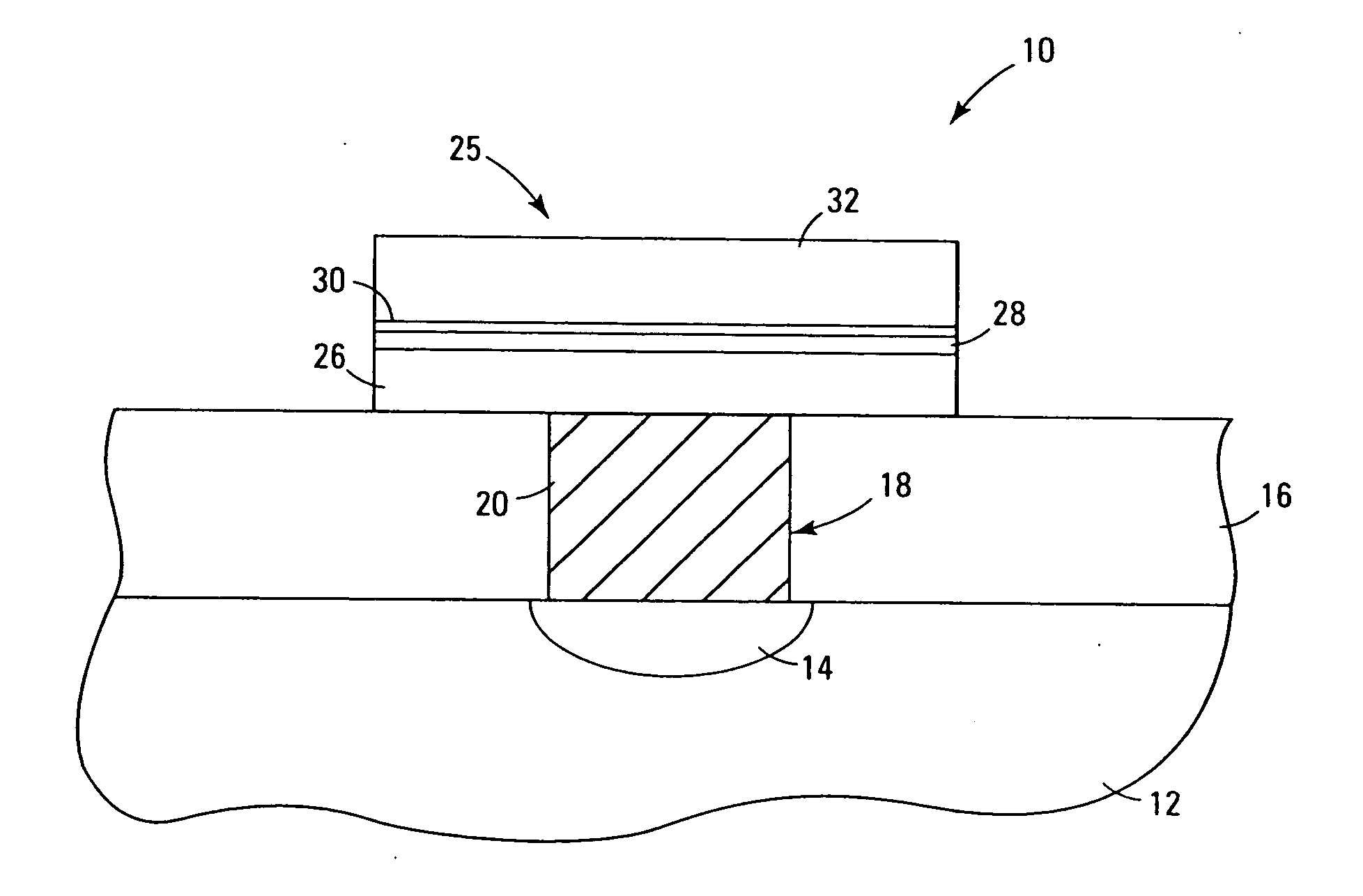
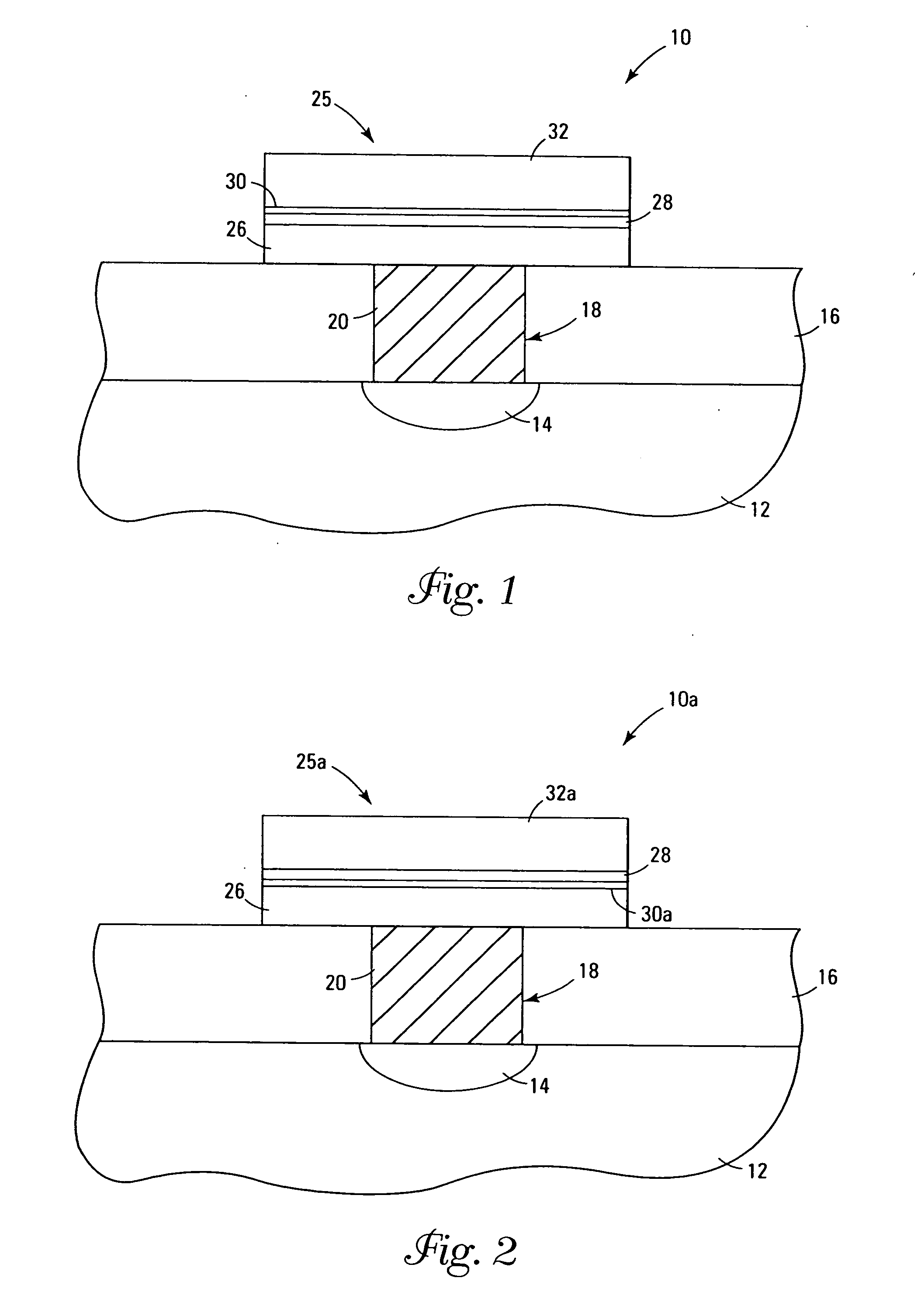
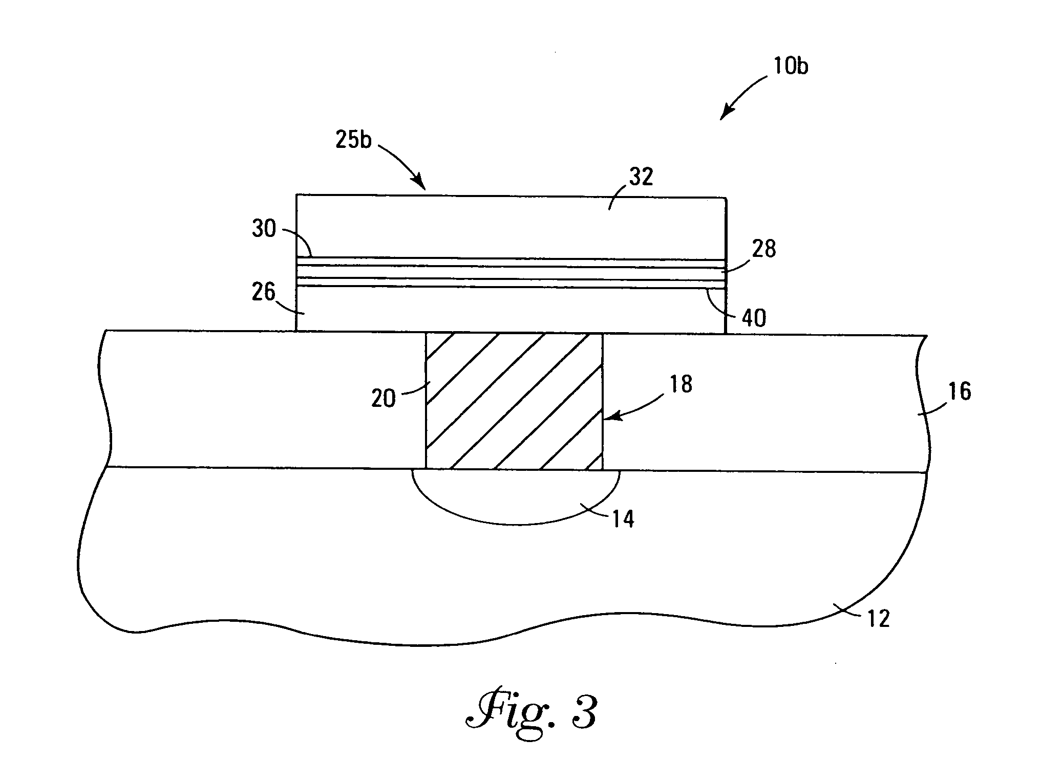
Image

Examples
example 1
Atomic Layer Deposition of Tantalum Pentoxide
[0068] Using an ALD process, precursor compounds tantalum pentafluoride, (TaF5), and 1,1,3,3-tetramethyldisiloxane, (CH3)2(H)Si—O—Si(H)(CH3)2, (both available from Sigma-Aldrich Chemical Co., Milwaukee, Wis.) were alternatively pulsed into a deposition chamber containing a platinum electrode having a surface temperature of about 260° C. After 800 cycles, a Ta2O5 layer having a thickness of 400 Å was achieved, the layer having no silicon or carbon contamination and a only trace of fluorine contamination (no more than 2 atom %) as determined by atomic emission spectroscopy (AES) analysis. X-ray diffraction analysis (XDA) showed the layer to be mainly amorphous with some (001) oriented hexagonal phase present, which remained the preferred crystalline orientation after the layer was annealed at 750° C. in an oxygen atmosphere.
[0069] A capacitor was formed by using physical vapor deposition to sputter platinum top electrodes through a hard m...
PUM
 Abstract
Description
Claims
Application Information