Self-assembly of organic-inorganic nanocomposite thin films for use in hybrid organic light emitting devices (HLED)
Inactive Publication Date: 2005-01-27
CANON KK
View PDF7 Cites 39 Cited by
Summary
Abstract
Description
Claims
Application Information
AI Technical Summary
This helps you quickly interpret patents by identifying the three key elements:
Problems solved by technology
Method used
Benefits of technology
Each method has advantages and disadvantages as outlined below.
Vacuum sublimation works well only with relatively low molecular weight (MW) compounds (<600 g/mol). Such compounds must be purified by sublimation or column chromatography to purities >99.99% prior to deposition to obtain superior light emitting efficiencies and device lifetimes. Vacuum sublimation allows for multi-layer configurations and very precise control of film thickness, both of which are advantageous in OLED processing. Drawbacks to vacuum sublimation are that it requires very costly equipment and it is limited to deposition on surface areas that are much smaller than surfaces that can be coated using spin coating. Additionally, device performance is adversely affected by the tendency of some sublimed compounds to crystallize with time. To prevent premature crystallization, compounds are currently being designed with high glass transition temperatures (Tgs) and substituents that minimize or prevent crystallization.
Dip coating, spin coating, spray coating, and printing techniques are generally applicable to the deposition of oligomeric and polymeric materials. It permits precise film thickness control, large area coverage and is relatively inexpensive compared to vacuum sublimation. Multi-layer configurations are only possible if the deposited layers are designed with curable functional groups for subsequent cross-linking, or with differing solub
Problems solved by technology
However, despite the enormous research and development effort on OLEDs, there are presently few commercially available products using this technology.
One of the apparent problems is the need for the development efficient materials to satisfy the electronic device requirements, especially lifetime.
Device stability, electronic efficiency, and manufacturing simplicity have been ongoing challenges in fabricating such devices.
Advances on OLED processing over the next two decades were limited to forming thin, light emitting films of organic compounds by vacuum deposition techniques, [Vincett, P. S.; Barlow, W. A.; Hann, R. A.; Roberts, G. G. Thin Solid Films 1982, 94, 476] and lowering driving voltages to <30V, however these single-layer devices suffered from both poor lifetimes and luminescence efficiencies.
Drawbacks to vacuum sublimation are that
Method used
Image
Click on the blue label to locate the original text in one second.
Reading with bidirectional positioning of images and text.
Examples
example 1
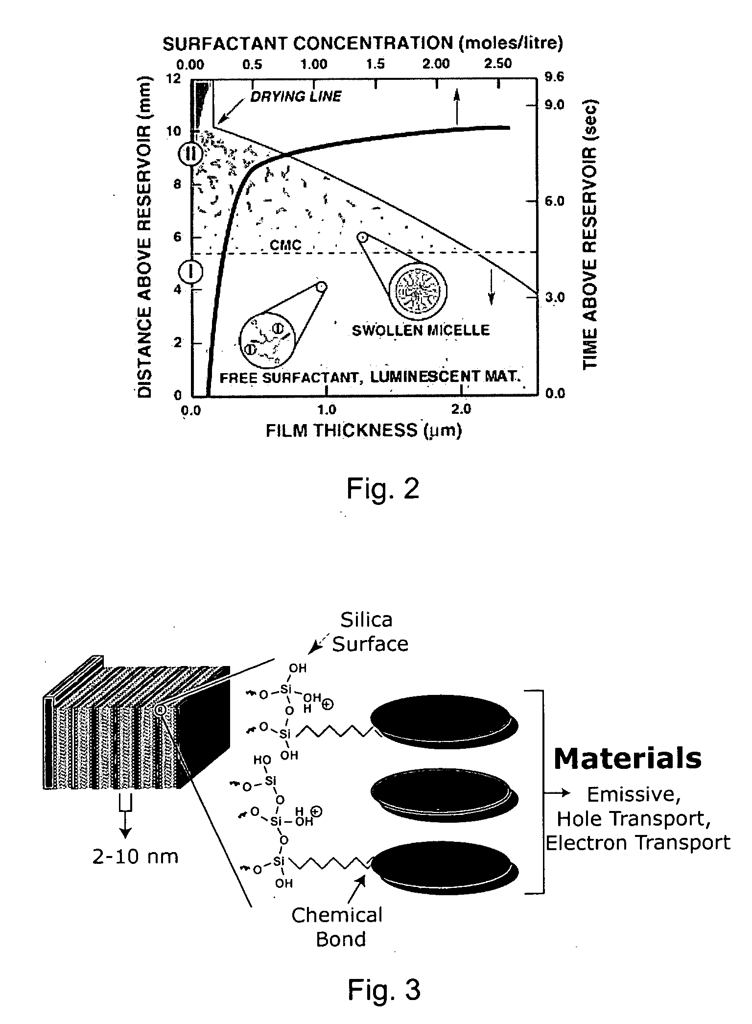
The initial silica precursor stock solution is prepared by refluxing TEOS (120 mL) [Si(OCH2CH3)4], THF (120 mL), water (9.8 mL), and 0.07N HCl (0.4 mL) at 60° C. for 90 minutes. This solution can be stored at −20° C. for 1 year. The acid concentration and reaction time are adjusted so as to minimize the size and condensation rate of the silica species. THF may also be replaced by ethanol, methanol, isopropanol, and aprotic solvents, such as diethylether, dioxane, N,N-dimethylformamide (DMF), N,N-dimethylacetamide (DMAC), N-methylpyrrolidone (NMP), dimethyl sulfoxide (DMSO), and acetone.
example 2
A portion of the silica precursor solution from Example 1 (17 mL) is diluted with THF (20 mL), followed by addition of water (0.7mL), 0.07N HCl (2.1 mL) and cetyltrimethylammonium bromide (CTAB, surfactant, 1.7 g). A hole transport material, N4′-(9,9-dimethyl-9H-fluoren-2-yl)-N4-(9,9-dimethyl-9H-fluoren-3-yl)-N4-phenyl-N4′-[4-(vinyltriethoxysilyl)-phenyl]-biphenyl-4,4′-diamine, (shown below, 1 g) dissolved in 20 mL THF is added to the solution with stirring followed by addition of 7-octenyltrimethoxysilane (silica coupling agent, 0.5 g).
The solution is stirred for 30 minutes. This solution is used immediately for deposition of thin films or stored at −20° C. where it is stable for up to 1 year.
example 3
A solution is prepared according to the procedure of Example 2, except the hole transport material is replaced by an electron transport material, 2-naphthalen-1-yl-5-[4-(3,3,3-vinyltriethoxysilyl)-phenyl]-[1,3,4]oxadiazole, (1 g), shown below.
PUM
Property
Measurement
Unit
Transparency
aaaaa
aaaaa
Transport properties
aaaaa
aaaaa
Luminescence
aaaaa
aaaaa
Abstract
A self-assembly process for preparing luminescent organic-inorganic nanocomposite thin films is disclosed. A homogeneous solution in water and an organic solvent is obtained containing a soluble silicate, a silica coupling agent, a surfactant, and an organic material having a hole transport, electron transport, and/or emissive material moiety. The silica coupling agent is selected to chemically react with the organic material. A film of the homogeneous solution is deposited onto a substrate. Preferentially evaporating the organic solvent enriches the concentration of water and non-volatile solution components to promote micelle formation. Organic materials migrate into the hydrophobic portion of the forming micelles. Continued evaporation promotes self-assembly of the micelles into interfacially organized liquid crystalline mesophases. Reacting the organic material and silica coupling forms a nanostructure self-assembly. Luminescent ordered nanocomposite structures prepared by the process, and organic-inorganic HLED devices fabricated from the luminescent organic-inorganic nanocomposite structures are disclosed.
Description
TECHNICAL FIELD A method is presented for producing new light emitting device material formed by the spontaneous evaporation-induced self-assembly of hole transport, electron transport, and emissive materials into layered organic / inorganic nanocomposite thin films. The thin films are deposited by dip-, spin-, or printing processes and form the layered material in less than 20 seconds. Subsequent curing by photo, thermal and / or chemical methods stabilizes the films for OLED application. BACKGROUND ART OLEDs Flat panel displays based on organic light emitting devices (OLEDs) have been studied extensively in recent years. OLEDs offer exceptional potential for thinner, more energy efficient displays with equal or better resolution and brightness compared to the current liquid crystal display (LCD) technology. OLEDs also offer high switching speeds, excellent viewing angles (>160°), red, green, and blue (RGB) color selection possibilities, and because no backlighting is necessary, ...
Claims
Application Information
Patent Timeline
Application Date:The date an application was filed.
Publication Date:The date a patent or application was officially published.
First Publication Date:The earliest publication date of a patent with the same application number.
Issue Date:Publication date of the patent grant document.
PCT Entry Date:The Entry date of PCT National Phase.
Estimated Expiry Date:The statutory expiry date of a patent right according to the Patent Law, and it is the longest term of protection that the patent right can achieve without the termination of the patent right due to other reasons(Term extension factor has been taken into account ).
Invalid Date:Actual expiry date is based on effective date or publication date of legal transaction data of invalid patent.