Circuit for reducing losses at light load in a soft switching full bridge converter

a converter and full bridge technology, applied in the direction of electric variable regulation, process and machine control, instruments, etc., can solve the problems of increasing unabated, higher switching losses, and worse electromagnetic interference (emi), so as to reduce component cost, reduce power loss, and provide design flexibility

Inactive Publication Date: 2005-02-10
ASTEC INT LTD
View PDF10 Cites 27 Cited by
  • Summary
  • Abstract
  • Description
  • Claims
  • Application Information

AI Technical Summary

Benefits of technology

[0021] An advantage of the present invention is that is provides design flexibility for practical applications.
[0022] Another advantage of the present invention is that it reduces the component cost since the ZVS inductor can be made using cheaper materials and dissipates lower power.
[0023] Another advantage of the present invention is that it lowers EMI at all load conditions.
[0024] Still another advantage of the present invention is that, unlike conventional ZVS converters, the value of the ZVS inductance reduces with increased operating frequency, thereby enabling higher density packaging by reducing component size.
[0025] Broadly stated, the present invention provides, in a DC-DC converter for providing substantially zero voltage switching (ZVS) having first and second input terminals to which an input DC voltage is coupled and two output terminals where the output DC power is provided, a bridge having a first and second switching leg, each leg comprising two controlled switches connected in series, each switch having a switch capacitance and a control input, each switching leg connected between the input terminals and having a junction point between its series-connected switches, a transformer having a primary winding and a secondary winding each having a first and second end, and a rectifier and output filter circuit coupled between the secondary winding and the output terminals, a circuit for reducing power losses at light loads and enabling very high frequency operation comprising a first inductor connected between the junction points for charging and discharging the switch capacitances; and a second inductor for providing high impedance to a sudden reversal of current having an end connected to the junction point of the first switching leg and another end connected to the first end of the primary winding, the second end of said primary winding is connected to the junction point of the second switching leg.
[0026] Broadly stated, the present invention also provides a DC-DC converter for providing substantially zero voltage switching (ZVS) having first and second input terminals to which an input DC voltage is coupled and two output terminals where the output DC power is provided comprising a bridge having a first and second switching leg, each leg comprising two controlled switches connected in series, each switch having a switch capacitance, each switching leg connected between the input terminals and having a junction point between its series-connected switches; a transformer having a primary winding and a secondary winding each having a first and second end; a rectifier and output filter circuit coupled between the secondary winding and the output terminals; a first and a second diode; a first inductor connected in series with the first diode between the junction points; and a second inductor connected in series with the second diode between the junction points; wherein the first diode has a cathode connected to an end of the first inductor and an anode connected to the junction point of the second switching leg and the second diode has a cathode connected to the anode of the first diode and an anode connected to an end of the second inductor; and a third inductor for providing high impedance to a sudden reversal of current having an end connected to the junction point of the first switching leg and another end connected to the first end of the primary winding, the second end of the primary winding is connected to the junction point of the second switching leg.

Problems solved by technology

Problems experienced with increasing the operating frequencies include higher switching losses and the generation of worse electromagnetic interference (EMI).
Since the switching losses in power semiconductors are directly proportional to the operating frequency, thermal management is also a big challenge, since the space saved by using smaller filtering components is more than offset by the need for larger heat sinks.
The demand for higher power density, however, is increasing unabated.
New problems are surfacing as the soft, ZVS converter is being switched at ever higher frequencies.
Conventional soft switching converters switching at high frequencies are exhibiting high power losses during light load conditions.
As a result, although such converters are very efficient at full load, they are prone to failure at light loads.
Many semiconductor manufacturers attribute this failure to various semiconductor phenomena, such as the reverse recovery speed of the MOSFET body diode, and the construction of the MOSFET's channel, etc.
One other significant problem, however, is that it is difficult to charge and discharge the output capacitance of the MOSFET bridge switching elements at light loads when the converter is in the hard switching mode.
This is because the energy stored in the resonant choke in such converters is very low and therefore cannot charge / discharge the output capacitance of the bridge switching elements.
This problem exists in all known ZVS control techniques.
In fact, this drawback at light load for conventional soft switching converters is even worse than for conventional hard switching bridge converters.
Since this current is typically very low, it cannot charge / discharge the MOSFET switch capacitance in the required delay time.
Since the energy stored in the magnetizing inductance is very low, it cannot enable ZVS of the bridge elements, and thus, can be neglected in the analysis.
Thus, there are two kinds of resistive losses in switch Qc: one due to the discharging of capacitor Cc and other due to the charging of capacitor Cd.
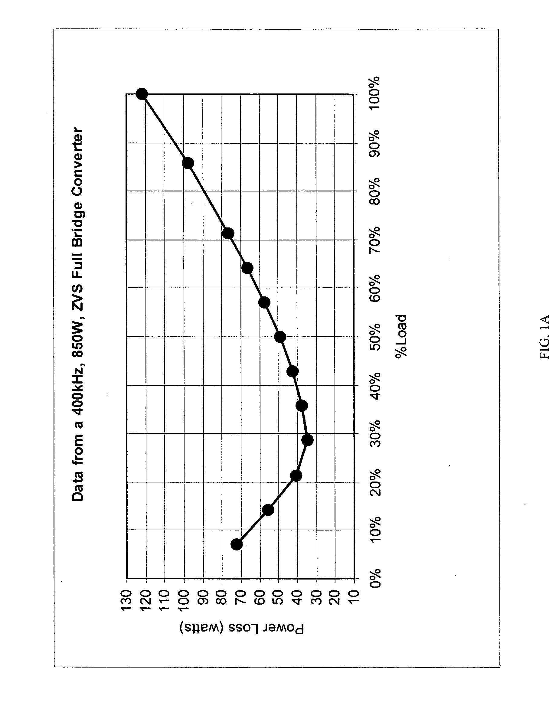
These resistive losses, and the resulting power dissipation, may be tolerable at lower switching frequencies in the range of 100 kHz to 200 kHz.
At much higher frequencies, e.g., above 400 kHz, however, these losses predominant such that the total power lost in the bridge switches at light loads exceeds the losses at full-load.
At light loads, most of this total loss is due to losses in the bridge switching devices.
In addition to the fact that the circuit topology in FIG. 2 has the drawback of losses at light load at higher frequencies, since the capacitance of each MOSFET switch is intrinsic and does not change with frequency, the size of the resonant inductor Lr is independent of frequency.
As a result it may be quite large for a high frequency power supply.
Inductor Lr is also lossy since it handles very high primary full load currents and its flux swings in both directions, generating high core losses.
This delay is a serious drawback at higher frequencies.
Although the circuit in FIG. 3 achieves ZVS action satisfactorily at higher loads, it still has the drawback of losses at light load at higher frequencies.
At frequencies above 200 kHz, for example, the core losses in the secondary side saturable cores of Ls1 and Ls2 are very high and could result in thermal runaway for the square loop amorphous cores typically used.
The blocking effect of these saturable inductors also reduces the available duty cycle.
However, this circuit has several drawbacks.
The ripple current stress on the capacitors can be significant, such that capacitors of higher cost are required.
The drawback of this solution is that this greater number of capacitors will occupy a larger volume, thereby creating an inefficient use of the available space.
Another drawback of the circuit in FIG. 4 is that any inequality between the values of C1 and C2 or between the values of Lr1 and Lr2 can create problems with the current mode control of the circuit.
Another drawback of this circuit is as follows.
This drawback is lessened in applications having a large transformer leakage inductance, but for transformers with very low leakage inductance, this problem in the converter 50 shown in FIG. 4 may result in some hard switching of one leg of the bridge.
Thus, at light loads, the dissipation in bridge switches is higher than at full-load and much less cooling air is available.
As a result, these devices may fail due to thermal runaway.
This cold plate approach is inefficient and cannot meet more demanding efficiency requirements at light load conditions.
The cold plate approach also complicates the construction of the power supply as several safety requirements must be met as well, e.g., requiring insulation on the secondary side, thus rendering this approach inconsistent with high density requirements.

Method used


Image

  • Circuit for reducing losses at light load in a soft switching full bridge converter
  • Circuit for reducing losses at light load in a soft switching full bridge converter
  • Circuit for reducing losses at light load in a soft switching full bridge converter

Examples


Embodiment Construction

[0046] A preferred embodiment of a circuit according to the present invention is shown at 100 in FIG. 5. Converter 100 includes a resonant inductor Lr and a blocking inductor Lblock as seen in FIG. 5. Resonant inductor Lr is connected across the output terminals of a bridge 110. Inductor Lr is parallel to the series combination of the transformer primary and a blocking inductor Lblock. A simplified representation of switches Qa, Qb, Qc, and Qd is shown in FIGS. 5-8 such that the switch capacitances of the corresponding switches are not shown. The existence of the switch capacitances is well known in the art. For reference, the switch capacitances are as shown in bridge 20 for switches Qa, Qb, Qc, and Qd in FIG. 1.

[0047] In operation, when a bridge diagonal, e.g., Qa, Qd, activates, current builds up through the primary winding after overcoming the blocking period of Lblock. At the same time, current builds up in Lr in the same direction, while storing energy therein. At the end of ...


PUM


Abstract

A circuit for reducing the internal power losses of a soft switching full bridge converter at light loads and enables very high frequency operation without using a cold plate approach. In a preferred embodiment, the circuit includes a resonant inductor and blocking inductor on the primary side of the converter arranged so as to provide the reduced losses for zero voltage switching bridge converter. The circuit provides the above benefits even for converters having a power transformer with very low leakage inductance. The circuit is not dependent on the presence of a high leakage inductance for the power transformer. The circuit can be used in soft switched half bridge or full bridge converters. The inventive circuit can also be used in a hard switching full bridge or half bridge converter for achieving zero voltage switching at reduced cost with reduced losses at light load, if the operating duty cycle of the converter is set near fifty percent.

Description

CROSS REFERENCE TO RELATED APPLICATION [0001] This application claims the benefit of U.S. Provisional Application No. 60 / 493,632, filed Aug. 9, 2003, which is incorporated by reference herein.FIELD OF INVENTION [0002] The present invention relates in general to power converter circuits and more particularly to zero voltage switching (ZVS) half bridge and full bridge converters and a circuit that reduces the high power loss at very light loads for such converters operating at high frequency. BACKGROUND OF INVENTION [0003] The modern technology trend is towards higher density and lower profile electrical devices. This trend has driven a demand for improving the power density of power supplies. As a result, various techniques have been developed to increase the switching frequencies of the power supply in order to reduce the size and bulk of magnetic components and filtering elements. Problems experienced with increasing the operating frequencies include higher switching losses and the...

Claims


Application Information

Patent Timeline
Patent Type & Authority Applications(United States)
IPC IPC(8): H02MH02M3/335H02M3/337
CPCH02M3/3376Y02B70/1491Y02B70/1433H02M2001/0048Y02B70/10H02M1/0032H02M1/0048H02M1/0058
Inventor PHADKE, VIJAY GANGADHARASUNCION, ARLAINDO VITUGBELTRAN, ISRAEL GOMEZ
Owner ASTEC INT LTD
Why Eureka
Try Eureka