Transfer film, method for forming metal back layer, and display device

a technology of metal back layer and transfer film, which is applied in the direction of thermography, electric discharge tube/lamp manufacture, and application of luminescent coatings, etc., can solve the problems of deteriorating the optical reflection performance of the metal back layer, difficult to keep the baking resistance characteristic in good condition, and conventional transfer methods that are difficult to put into actual use. achieve the effect of high resistan

Inactive Publication Date: 2005-03-24
KK TOSHIBA +2
View PDF1 Cites 5 Cited by
  • Summary
  • Abstract
  • Description
  • Claims
  • Application Information

AI Technical Summary

Benefits of technology

[0011] The present invention has been completed to remedy the above problems, and it is an object of the invention to provide a transfer film capable of forming a metal back layer having good characteristics by a transfer method, a method for forming the metal back layer having remarkable advantageous effects efficiently by the transfer method, and a display device which has a high metal back effect and a remarkable withstand voltage characteristic and can make display with high luminance and high quality.

Problems solved by technology

But, such characteristics were hardly realized at the same time and the transfer method was conventionally hard to put into actual use.
Therefore, the decomposition gas generated at this time causes destruction of the metal film such as a blister, and it is difficult to keep the baking resistance characteristic in good condition.
But, such methods had a disadvantage that a side effect was caused to deteriorate the optical reflection performance of the metal back layer.
But, this method is also hard to form a good metal film.
Besides, in the aforementioned lacquer method for forming a metal back layer a metal film is formed on a base surface having large projections and depressions by vacuum deposition, so that it is hard to form a thin film having high reflectance.
Therefore, it was hard to obtain a phosphor screen having high luminance, and especially there was a problem of unevenness in luminance on the phosphor screen of the display such as the FED which operates in a low energy electron beam region.
Furthermore, the FED has a gap (space) of about one to several mm between the face plate having the phosphor screen and the rear plate having the electron-emitting element, and the gap cannot be increased in view of resolution and characteristics of a spacer.
As a result, a high voltage of about 10 kV is applied to generate a strong electric field in the very small gap between the face plate and the rear plate, resulting in a problem that an electric discharge (dielectrical breakdown) tends to be caused.
And, the occurrence of an electric discharge had a tendency of destroying or degrading the electron-emitting element or the phosphor screen.

Method used


Image

  • Transfer film, method for forming metal back layer, and display device
  • Transfer film, method for forming metal back layer, and display device
  • Transfer film, method for forming metal back layer, and display device

Examples


first embodiment

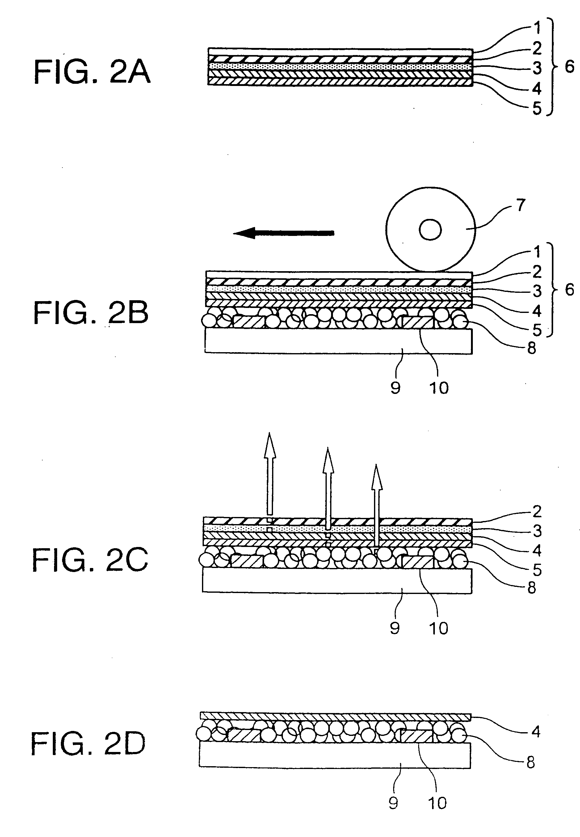
[0076]FIG. 7 is a sectional diagram showing the transfer film of the invention. In the drawing, reference numeral 11 denotes a base film, on which a parting-agent layer 12, a protective film 13, a metal film 14 and an adhesive-agent layer 15 are stacked in order.

[0077] The base film 11 is not particularly limited but can be made of a resin selected from polyester (polyethylene terephthalate, polybutylene terephthalate), polyethylene, polypropylene, nylon (polyamide), cellophane, polycarbonate, polyacrylate, polyimide and aromatic polyamide which are generally used as a base film. This base film 11 desirably has a thickness of about 5 to 50 μm. If the base film 11 is excessively thin, deformation is excessive and wrinkles etc. are easily generated in the metal film 14 when the transfer film is under the pressing treatment. And, if it is excessively thick, followability for the base is deteriorated, and the transfer property is lowered.

[0078] As a parting agent, cellulose acetate, wa...

second embodiment

[0089] Then, the transfer film according to the present invention will be explained. As shown in FIG. 8, the transfer film has the parting-agent layer 12 formed on the base film 11, a high resistance layer 16 having a surface resistivity of 102 to 108 Ω / □ and the adhesive-agent layer 15 are stacked on it. It may also be configured to have the protective film between the parting-agent layer 12 and the high resistance layer 16. The high resistance layer 16 is desired to have a thickness of 5 to 150 nm, and more preferably in a range of 10 to 100 nm.

[0090] The material for the high resistance layer 16 can be many kinds of inorganic materials such as aluminum oxide, silicon dioxide (SiO2), AlN and TiN. The following method can be adopted to form the high resistance layer of an aluminum oxide in the transfer film.

[0091] Specifically, a degree of vacuum of about 1×10⁻⁴ Pa is provided, and by depositing aluminum on the parting-agent layer or the protective film while introducing oxygen th...

third embodiment

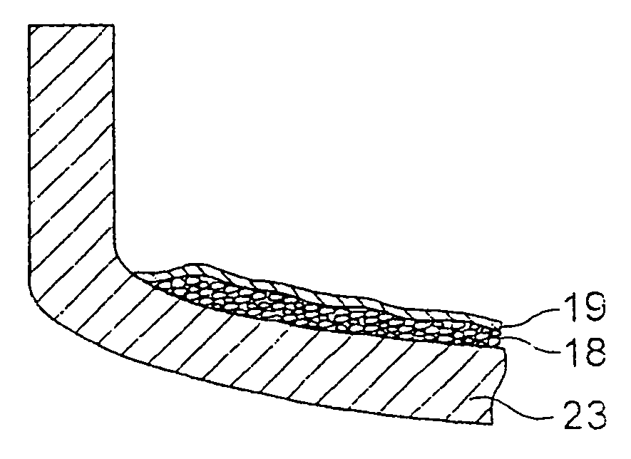
[0098] Next, the transfer film according to the present invention will be explained. As shown in FIG. 12, in the transfer film, the parting-agent layer 12 is formed on the base film 11, and a transfer layer 20 for forming a metal back and the adhesive-agent layer 15 are stacked on it. The transfer layer 20 has a two-layer structure in which a low resistance layer 22 having a surface resistivity of less than 102 Ω / □ and good reflectiveness is stacked on a high resistance layer 21 having a surface resistivity of 102 to 108 Ω / □. The transfer layer 20 having the above two-layer structure is desired to have a total thickness of 5 to 150 nm, and more preferably in a range of 10 to 100 nm.

[0099] The above transfer film is used to form a phosphor screen having a metal back as shown in FIG. 13. On this phosphor screen, the metal back layer 19, which is comprised of the low resistance layer 22 having a surface resistivity of less than 103 Ω / □ and good reflectiveness and the high resistance la...


PUM

PropertyMeasurementUnit
resistanceaaaaaaaaaa

Abstract

A transfer film comprising a base film (11), a parting-agent layer (12), a protective film (13), and a metal film (14), the latter three being formed on the base film (11) in order, wherein the protective film (13) contains a softening agent such as a phosphate, an aliphatic monobasic acid ester, an aliphatic dibasic acid ester, or a dihydric alcohol ester. By using such a transfer film, a metal back layer is formed. Since the transfer layer of the transfer film has a surface resistivity of as high as 102-108 Ω / , the surface resistivity of the formed metal back layer is high, and discharge is suppressed.

Description

TECHNICAL FIELD [0001] The present invention relates to a transfer film, a method for forming a metal back layer of a phosphor screen by using the transfer film, and an display device having the metal back layer. BACKGROUND ART [0002] Conventionally, for the phosphor screen of a cathode ray tube (CRT), a field emission type display (FED) and the like, a metal back type structure in which a metal film is formed on the inner surface (surface opposite to a face plate) of a phosphor layer is adopted extensively. In the light emitted from a phosphor by the electrons discharged from an electron source, this metal back layer reflects the light, which advances toward the electron source, to the face plate side to improve luminance and to stabilize the potential of the phosphor layer. It also has a function to prevent the phosphor layer from being damaged by ions which are generated when the gas remaining in a vacuum envelop is ionized. [0003] The metal back layer is conventionally formed by...

Claims


Application Information

Patent Timeline
Patent Type & Authority Applications(United States)
IPC IPC(8): H01J29/28
CPCH01J29/28H01J31/123Y10T428/253Y10T428/265Y10T428/1476H01J2329/28Y10T428/31692Y10T428/31681H01J9/22
Inventor ITO, TAKEOTANAKA, HAJIMENAKAZAWA, TOMOKONAKAYAMA, TAICHIROSHINOHARA, TAKAAKINAKAYAMA, YOICHIROSAKAI, KAZUO
Owner KK TOSHIBA
Why Eureka
Try Eureka