Silicon-based thin-film photoelectric conversion device and method of manufacturing thereof

a technology of photoelectric conversion device and thin film, which is applied in the manufacture of final products, basic electric elements, coatings, etc., can solve the problems of increasing the cost of adding the production cost of solar cells to the cost of key equipment used in the process of manufacturing devices, increasing the cost of cvd equipment for example, and achieving excellent performance and quality, simple manufacturing equipment, and low cost

Inactive Publication Date: 2005-04-21
SHARP KK
View PDF1 Cites 21 Cited by
  • Summary
  • Abstract
  • Description
  • Claims
  • Application Information

AI Technical Summary

Benefits of technology

[0010] An object of the present invention is to provide a method of manufacturing a silicon-based thin-film photoelectric conversion device having excellent performance and quality with a simple manufacturing apparatus at a low cost and a high efficie

Problems solved by technology

Key apparatuses used in the process of manufacturing the devices, CVD apparatus for example, are increasing in cost to add the production cost of the solar cells.
The increased cost is thus one of factors that hinder large-scale and widespread use of the solar cells.
Regarding the inline system, however, the substrate is transported linearly, which means that the whole apparatus has to be stopped even if only a part of the apparatus fails to need maintenance.
Therefore, a disadvantage of the inline system is that, even if one film deposition chamber for forming i-layers requires maintenance, the entire manufacturing line has to be stopped.
The manufacturing apparatus of the multi-chamber system, however, has a plurality of lines along which the substrate is transported via the intermediate chamber, resulting in an inevitable increase in complexity of the mechanical structure of the intermediate chamber.
For example, the mechanism for maintaining the airtightness between the intermediate chamber and each of the deposition chambers while transporting the substrate is complicated to increase th

Method used


Image

  • Silicon-based thin-film photoelectric conversion device and method of manufacturing thereof
  • Silicon-based thin-film photoelectric conversion device and method of manufacturing thereof
  • Silicon-based thin-film photoelectric conversion device and method of manufacturing thereof

Examples


example 1

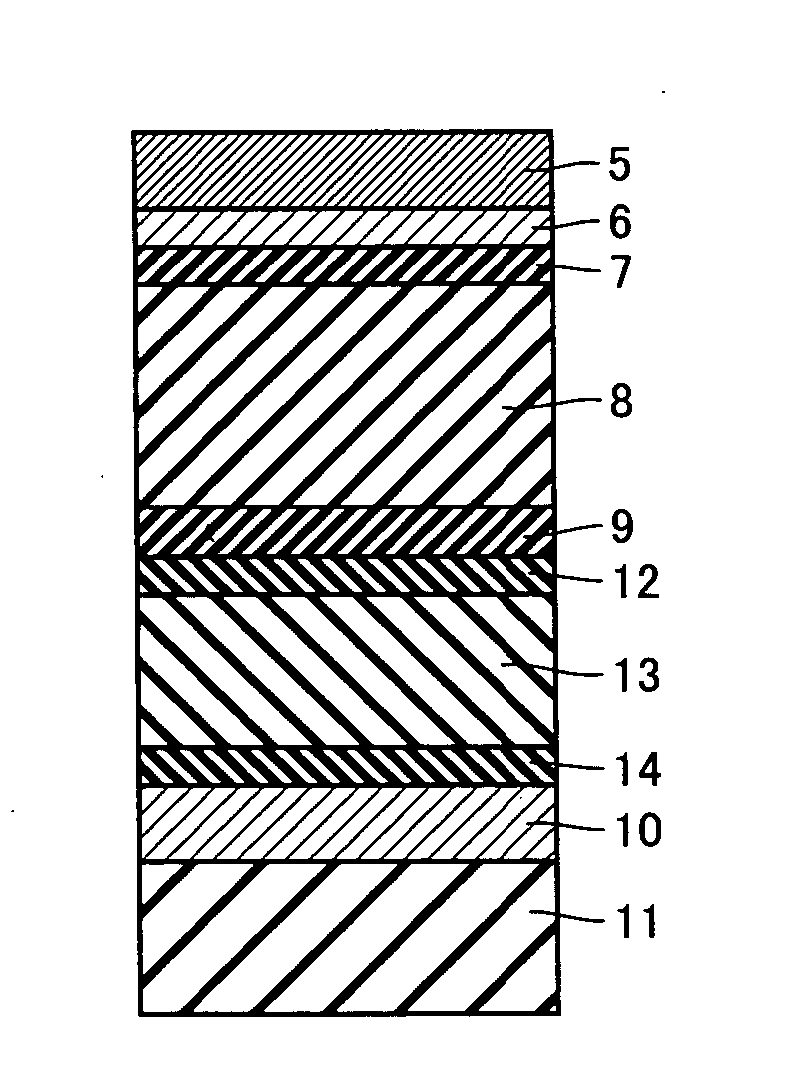
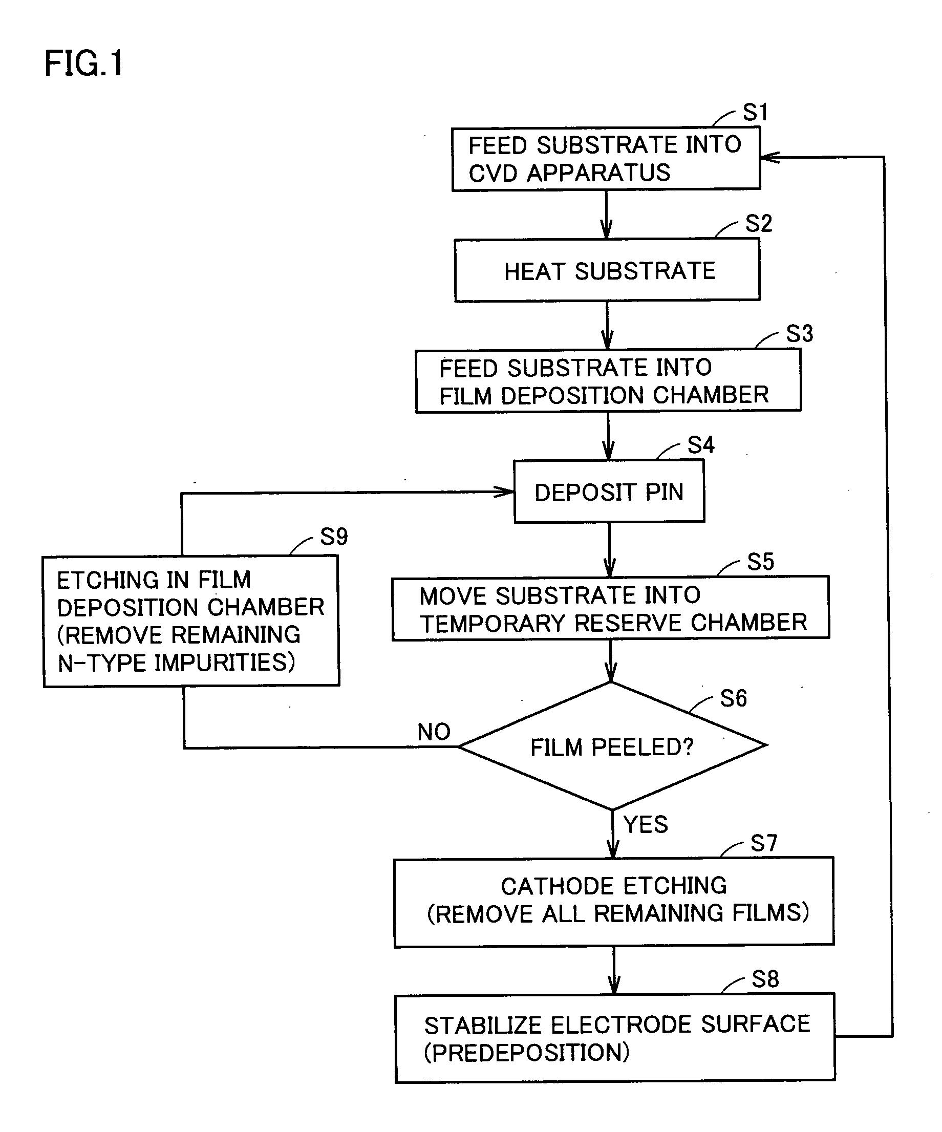
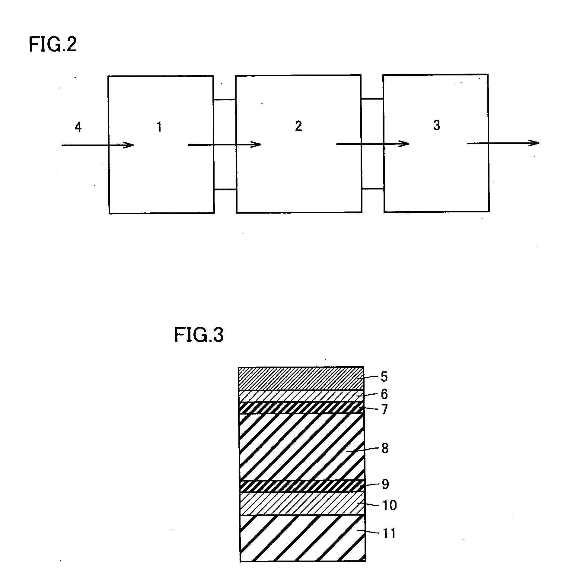
[0040] In Example 1, silicon-based thin-film photoelectric conversion devices having the structure shown in FIG. 3 were successively manufactured through the manufacturing process repeated multiple times. A first silicon-based thin-film photoelectric conversion device was manufactured by forming transparent conductive film 10 of SnO2 on substrate 11 of glass and thereafter depositing boron-doped p-type semiconductor layer 9 of microcrystalline silicon with a thickness of 10 nm, non-doped i-type photoelectric conversion layer 8 of microcrystalline silicon with a thickness of 3 μm and phosphorus-doped n-type semiconductor layer 7 of silicon with a thickness of 20 nm in this order on transparent conductive film 10. Further, on n-type semiconductor layer 7, conductive film 6 of ZnO with a thickness of 50 nm and metal electrode 5 of Ag with a thickness of 300 nm were formed so that a back electrode unit comprised of conductive film 6 and metal electrode 5 was provided.

[0041] In this exa...

example 2

[0046] Deposition of pin layers was successively done approximately 50 times under the conditions employed in Example 1 and consequently the total thickness of films remaining impurities stacked on the cathode reached 150 μm or more. Point detects due to peeling of the remaining films on the cathode were likely to occur and accordingly it was found that the manufacturing yield of photoelectric conversion devices decreases to 30% or lower. After the yield deterioration due to the peeling of remaining films was confirmed, the remaining films on the cathode were removed under the same conditions as the cleaning conditions used in removing remaining n-type impurities in the film deposition chamber in Example 1. Specifically, as an etching gas and a diluent gas, nitrogen trifluoride and argon gas of 20 volume % in concentration were supplied and etching was done under a pressure of 67 Pa. The resultant etch rate was 10 nm / s or higher so that all the stacked films with a thickness of 150 ...

example 3

[0047] On a photoelectric conversion device including an amorphous silicon-based photoelectric conversion layer, a photoelectric conversion device including a microcrystalline silicon-based photoelectric conversion layer that was firstly produced by a similar method to that in Example 1 was stacked to produce a stacked photoelectric conversion device having the structure as shown in FIG. 5. The photoelectric conversion efficiency of the stacked photoelectric conversion device was measured in a similar manner to that in Example 1 and the measurement was 12.5%. After this, by a method similar to that in Example 1, the cleaning process was followed for removing remaining n-type impurities. Then, a photoelectric conversion device having a microcrystalline silicon-based photoelectric conversion layer that was secondly produced was obtained. This photoelectric conversion device was then stacked on a photoelectric conversion device including an amorphous silicon-based photoelectric convers...


PUM

PropertyMeasurementUnit
Temperatureaaaaaaaaaa
Lengthaaaaaaaaaa
Lengthaaaaaaaaaa

Abstract

An excellent silicon-based thin-film photoelectric conversion device is manufactured simply and efficiently at a low cost. Specifically, a method of manufacturing the silicon-based thin-film photoelectric conversion device including a p-type semiconductor layer, an i-type microcrystalline silicon-based photoelectric conversion layer and an n-type semiconductor layer deposited by plasma CVD includes the steps of: successively depositing the p-type semiconductor layer, the i-type microcrystalline silicon-based photoelectric conversion layer and the n-type semiconductor layer on a substrate within the same plasma CVD film deposition chamber; transferring the substrate out of the film deposition chamber; and subsequently to the step of depositing the p-type semiconductor layer, the i-type microcrystalline silicon-based photoelectric conversion layer and the n-type semiconductor layer, eliminating influences of remaining n-type impurities on a cathode and/or within the film deposition chamber.

Description

[0001] This nonprovisional application is based on Japanese Patent Application No. 2003-358091 filed with the Japan Patent Office on Oct. 17, 2003, the entire contents of which are hereby incorporated by reference. BACKGROUND OF THE INVENTION [0002] 1. Field of the Invention [0003] The present invention relates to a method of manufacturing a silicon-based thin-film photoelectric conversion device having excellent performance. In particular, the present invention relates to a silicon-based thin-film photoelectric conversion device dramatically improved in production cost and production efficiency. [0004] 2. Description of the Background Art [0005] In recent years, development of and increased production volume of solar cells using thin films containing such a crystalline silicon as polycrystalline silicon or microcrystalline silicon for example have received worldwide attention. A significant feature of this type of solar cells is in that reduction in cost and improvements in perform...

Claims


Application Information

Patent Timeline
IPC IPC(8): H01L21/00H01L31/04H01L31/075H01L31/077H01L31/18
CPCH01L31/077Y02E10/545H01L31/1824Y02E10/547Y02E10/548Y02P70/50
Inventor KISHIMOTO, KATSUSHIFUKUOKA, YUSUKENOMOTO, KATSUHIKO
Owner SHARP KK
Why Eureka
Try Eureka