

GaN-based III - V group compound semiconductor device and p-type electrode for the same
a compound semiconductor and gan-based technology, applied in semiconductor lasers, semiconductor/solid-state device details, lasers, etc., can solve the problem of not having a sufficiently low specific contact resistance of ohmic contact materials, and achieve excellent electrical, optical, and thermal characteristics.
- Summary
- Abstract
- Description
- Claims
- Application Information
AI Technical Summary
Benefits of technology
Problems solved by technology
Method used
Image

Examples
embodiment 1
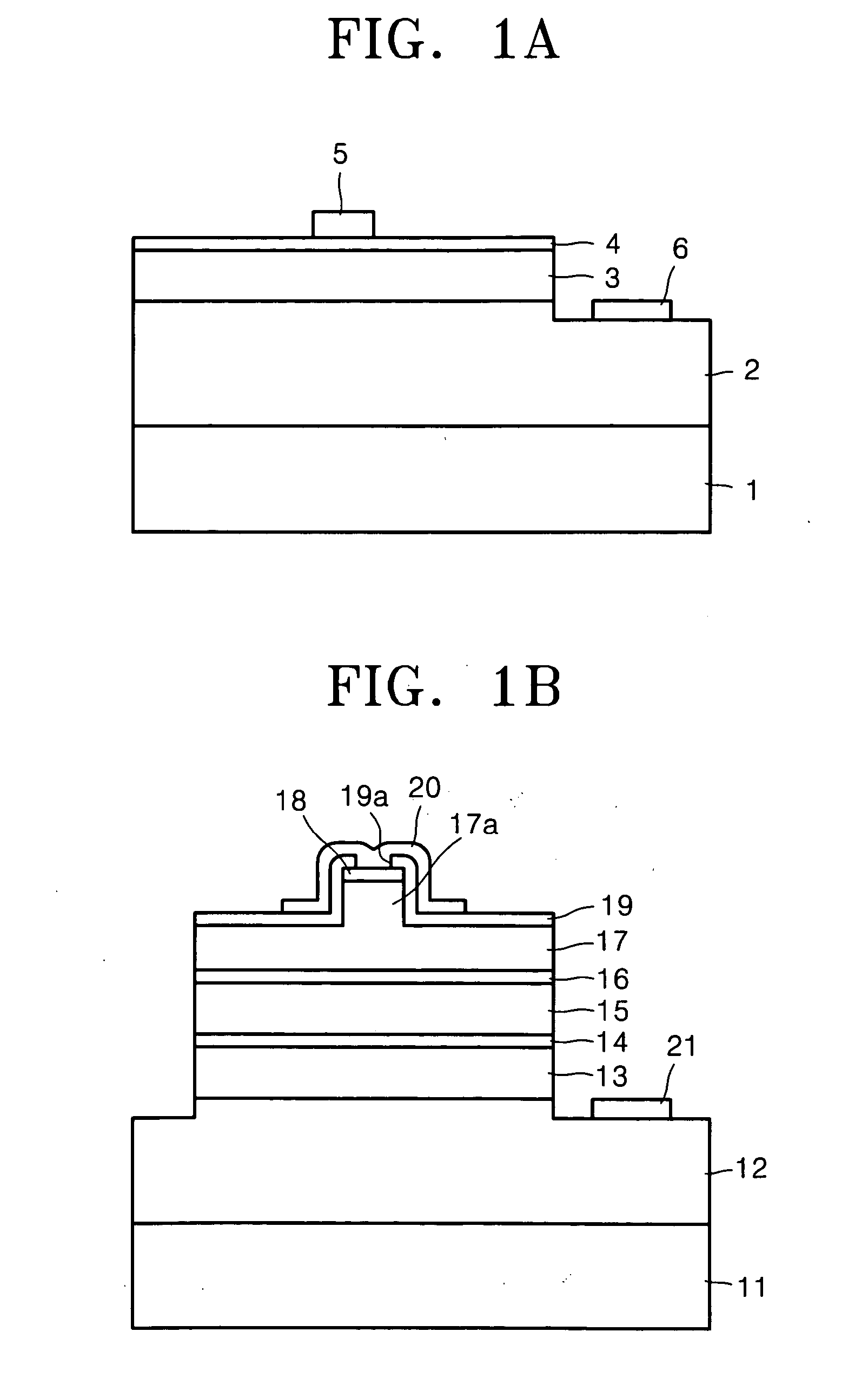
[0058] In operation 1, at the outset, the surface of a sample, in which a GaN-based semiconductor crystalline layer including a p-type semiconductor layer is formed on a substrate, is washed in an ultrasonic bath at a temperature of 60° C. using trichloroethylene (TCE), acetone, methanol, and distilled water, respectively, for 5 minutes each time. Then, the resultant structure is hard baked at a temperature of 100° C. for 10 minutes to remove the remaining moisture from this sample.
[0059] In operation 2, a photoresist layer is spin-coated on the p-type compound semiconductor layer at 4,500 RPM, and the resultant structure is soft baked at a temperature of 85° C. for 15 minutes.
[0060] In operation 3, to develop a mask pattern, the sample is aligned with a mask, exposed to ultraviolet rays (UV) of 22.8 mW, and dipped in a solution containing a mixture of a developing solution with distilled water in a ratio of 1:4 for 25 seconds.
[0061] In operation 4, the developed sample is dipped...
embodiment 2
[0064] In operation 1′, operations 1 through 4 of the first embodiment are performed in the same manner.
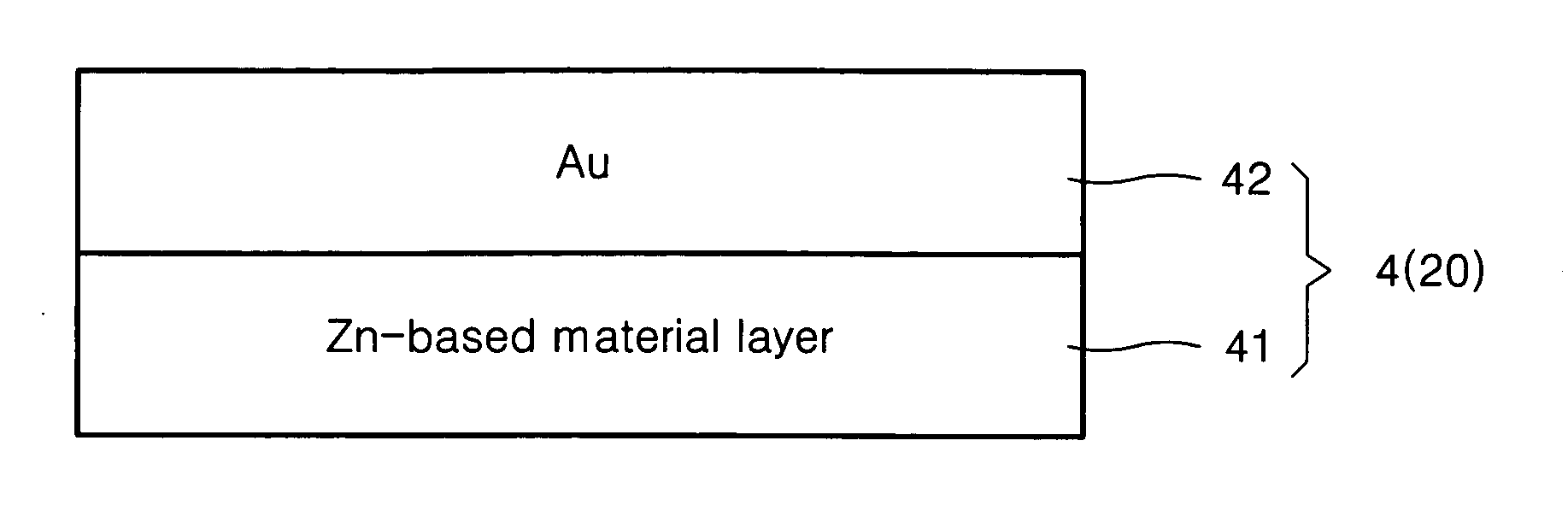
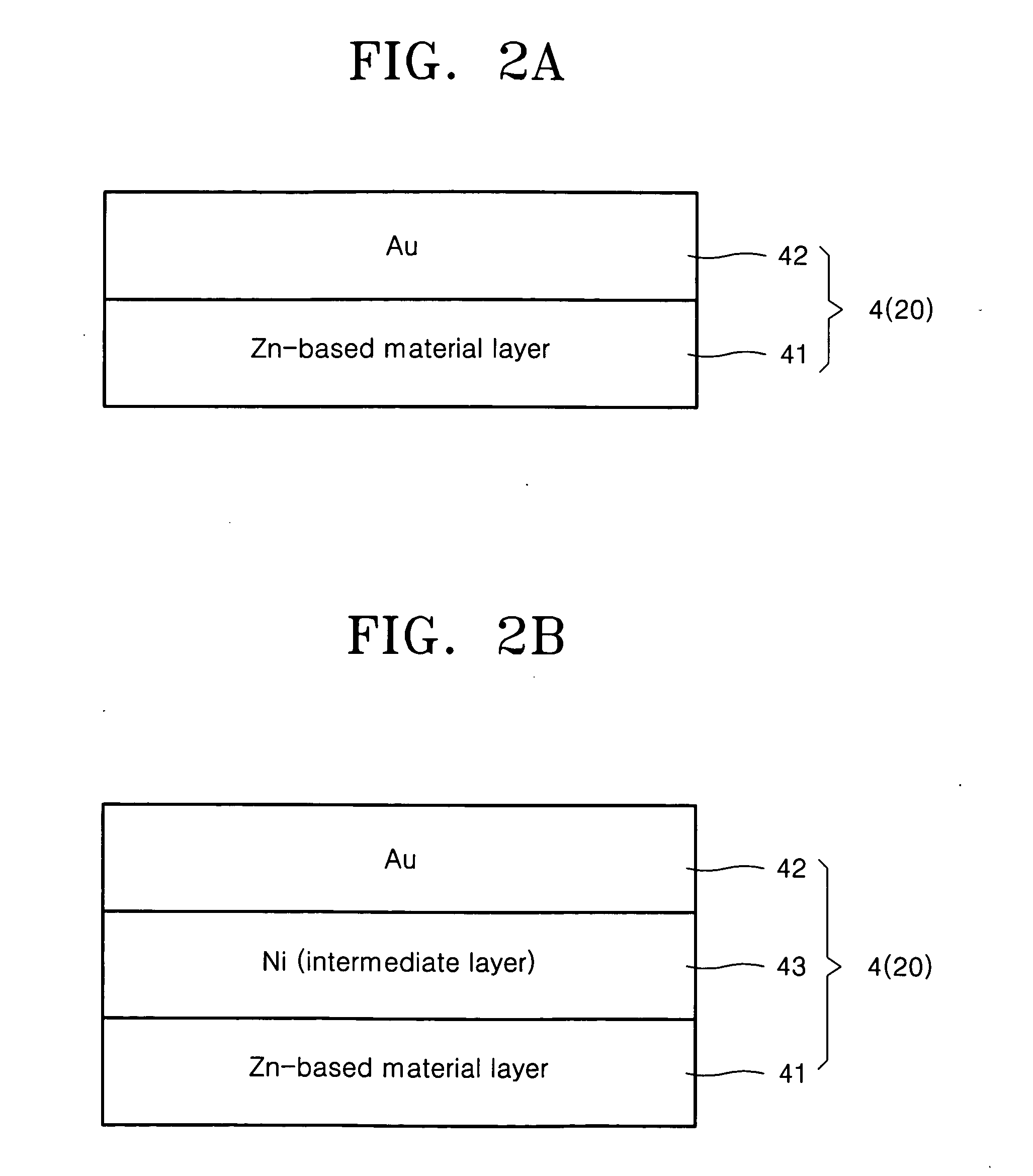
[0065] In operation 2′, a Zn—Ni alloy (10 nm) / Au (10 nm) according to the present invention is deposited on the entire surface of the resultant structure using an e-beam evaporator, and lift-off is carried out using acetone to pattern an electrode.
[0066] In operation 3′, the sample is loaded into an RTA furnace and annealed in an air atmosphere at a temperature of about 350 to 550° C. for 1 minute. As a result, a transparent electrode is formed on the surface of the p-type semiconductor layer disposed on the substrate.
embodiment 3
[0067] In operation 1″, operations 1 through 4 of the first embodiment are performed in the same manner.
[0068] In operation 2″, a Zn—Ni alloy (3 nm) / Ni (2 nm) / Au (5 nm) according to the present invention is deposited on the entire surface of the resultant structure using an e-beam evaporator, and lift-off is carried out using acetone to pattern an electrode.
[0069] In operation 3″, the sample is loaded into an RTA furnace and annealed in an air atmosphere at a temperature of about 350 to 550° C. for 1 minute. As a result, a transparent electrode is formed on the surface of the p-type semiconductor layer disposed on the substrate.
[0070] As described above, the present invention provides an ohmic electrode forming process, which is one of the most important techniques that enhance commercial availability of LEDs and LDs using p-type GaN-based semiconductor. Thus, GaN-based semiconductor becomes highly commercially available. Also, since the surface of an electrode is in a very good ...
PUM
 Abstract
Description
Claims
Application Information