Plasma enhanced ALD of tantalum nitride and bilayer

a technology of tantalum nitride and enhanced ald, which is applied in the direction of plasma technique, semiconductor/solid-state device details, superimposed coating process, etc., can solve the problems of low the use of pvd technologies for these layers is not expected to be applicable for technologies using nodes less than approximately 45, and the failure of ald of ta and tan as a bilayer is only rar

Inactive Publication Date: 2005-05-05
GLOBALFOUNDRIES INC
View PDF9 Cites 27 Cited by
  • Summary
  • Abstract
  • Description
  • Claims
  • Application Information

AI Technical Summary

Benefits of technology

[0005] It is therefore an aspect of the present invention to provide a method for producing a copper diffusion barrier that is reliable.
[0007] The present invention is directed to a novel and simple method for depositing a tantalum nitride layer with controllable nitrogen content and a tantalum nitride / tantalum barrier using PE-ALD. Low resistivity cubic tantalum nitride thin films may be grown by plasma-enhanced atomic layer deposition (PE-ALD) using a tantalum halide, such as TaCl5 as the metal precursor and a hydrogen / nitrogen plasma. The deposition can be performed by alternate exposures of TaCl5 and a plasma composed of a mixture of hydrogen and nitrogen or the consecutive exposure of hydrogen plasma and nitrogen plasma. The nitrogen content in the films can be controlled from a nitrogen to tantalum ratio of 0 up to 1.7 by changing nitrogen partial pressure during the second, reactant step of the ALD sequence. A bilayer (or multilayer) of tantalum nitride / tantalum can be deposited by simply switching off the nitrogen flow following the deposition of tantalum nitride. This bilayer shows good copper diffusion barrier properties.

Problems solved by technology

However, for successful implementation of copper interconnect technology, proper diffusion barrier materials with high thermal stability, low resistivity, and low reactivity with copper are essential since copper has higher diffusivity than aluminum and copper easily diffuses through dielectrics, producing deep level defects which are detrimental to the performance of CMOS transistors.
However, the use of PVD technologies for these layers is not expected to be applicable for technologies using nodes smaller than approximately 45 nanometers due to limited ability of the deposited films to conform to these smaller features.
While it is possible to deposit metallic Ta films using ALD with a halide tantalum precursor, the ALD of Ta and TaN as a bilayer has been only rarely successful for two reasons.
First, the conventionally available ALD of TaN using an inorganic source (such as TaCl5), reacted with ammonia (NH3) has been reported to produce a highly resistive phase of tantalum nitride, the Ta3N5 phase, which presents practical difficulties for the use of these films as barriers in conducting circuits.
Second, while it is possible to deposit TaN films using a metal-organic Ta source such as, for example, TBTDET (tertbutylimidotris(diethylamido)tantalum), it is impossible to use this precursor for the deposition of a metallic Ta film by ALD since the TaN bond cannot be reduced in this chemical system.

Method used


Image

  • Plasma enhanced ALD of tantalum nitride and bilayer
  • Plasma enhanced ALD of tantalum nitride and bilayer
  • Plasma enhanced ALD of tantalum nitride and bilayer

Examples


example

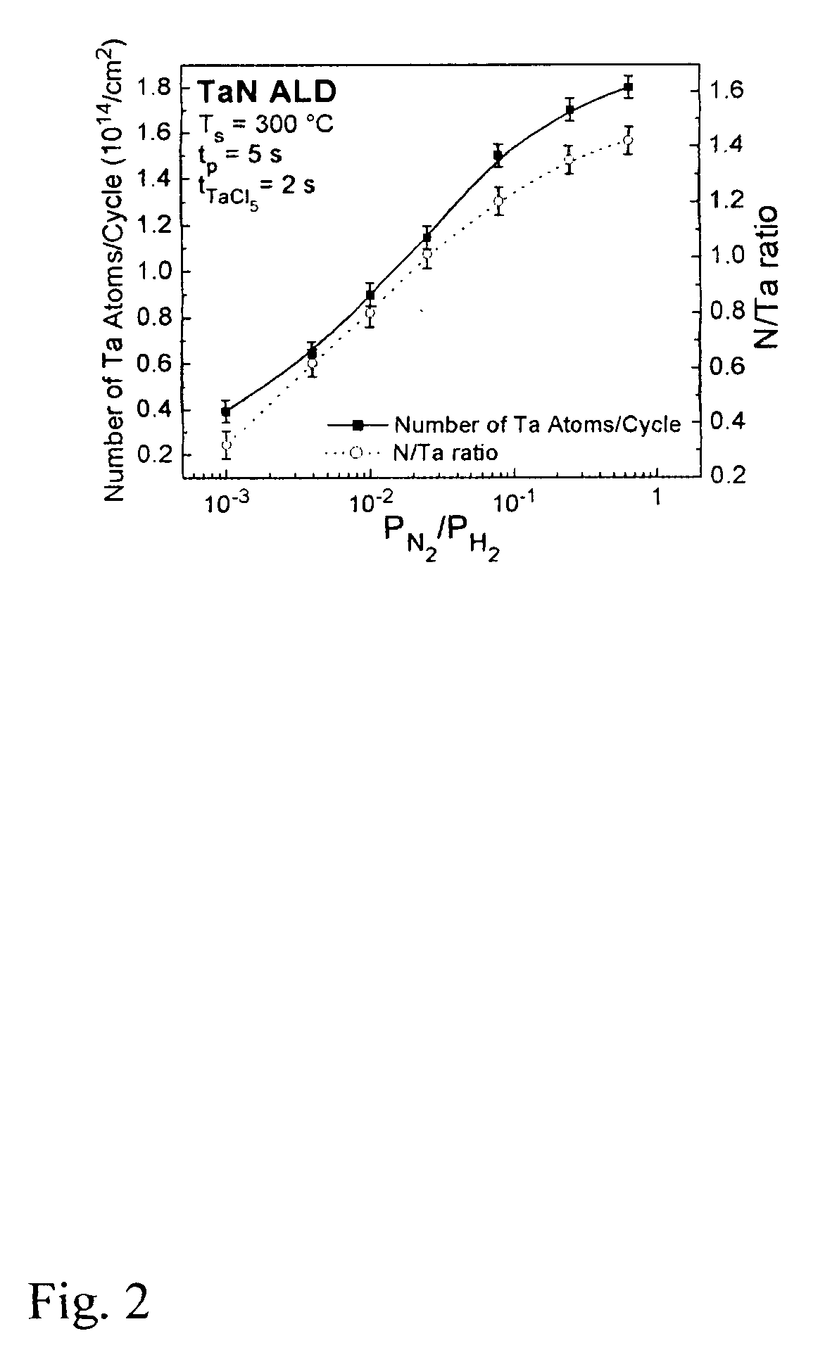
[0030] Tantalum nitride films are grown typically with TaCl5 exposure time of 2 seconds and plasma exposure time of 5 seconds, which correspond to saturation condition of ALD. This saturation is due to the self-limited adsorption of the precursor. The total time for one cycle is typically 12 seconds including the evacuation time after TaCl5 and plasma exposures. The hydrogen partial pressure during exposure is set as 2.5×10⁻³ Torr and nitrogen partial pressure is changed. The total pressure (argon and TaCls vapor) during TaCl5 exposure is constant at 3.0×10⁻² Torr. A typical number of cycles is 50-800 to produce tantalum nitride films with thicknesses in the range of 20 to 400 Angstroms, depending upon growth conditions.

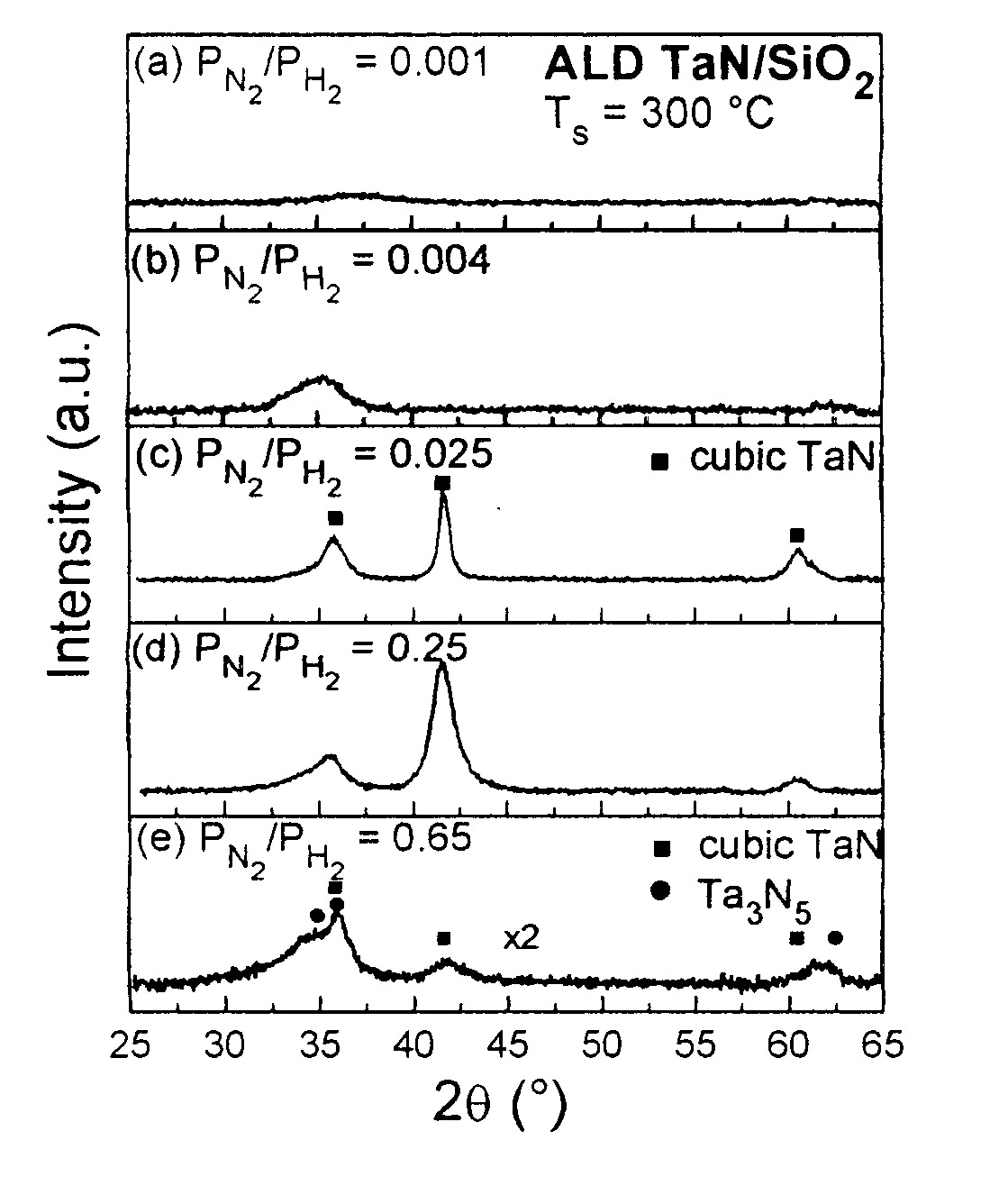
[0031]FIG. 1 illustrates X-ray diffraction (XRD) results of PE-ALD TaNx grown at Ts=300° C. At low nitrogen partial pressure (nitrogen to hydrogen partial pressure ratio=0.001), the XRD spectrum shows a broad peak at approximately 2θ=38°. For a higher partial pressu...


PUM

PropertyMeasurementUnit
temperatureaaaaaaaaaa

Abstract

A method to deposit TaN by plasma enhanced layer with various nitrogen content. Using a mixture of hydrogen and nitrogen plasma, the nitrogen content in the film can be controlled from 0 to N / Ta=1.7. By turning off the nitrogen flow during deposition of TaN, a TaN / Ta bilayer is easily grown, which has copper diffusion barrier properties superior to those of a single Ta layer or a single TaN layer.

Description

FIELD OF THE INVENTION [0001] This invention relates to electrical interconnection structures. More particularly, it relates to “back end of the line” (BEOL) interconnections in high performance integrated circuits, and diffusion barriers used in such devices. BACKGROUND OF THE INVENTION [0002] In view of the fact that copper has higher electromigration resistance, and thus reliability, as well as higher conductivity than aluminum wiring, copper interconnects are being widely accepted as standard interconnect technology in semiconductor device fabrication. However, for successful implementation of copper interconnect technology, proper diffusion barrier materials with high thermal stability, low resistivity, and low reactivity with copper are essential since copper has higher diffusivity than aluminum and copper easily diffuses through dielectrics, producing deep level defects which are detrimental to the performance of CMOS transistors. It is for this reason that a thin tantalum / ta...

Claims


Application Information

Patent Timeline
Patent Type & Authority Applications(United States)
IPC IPC(8): B32B9/00C23C16/50C23C16/08C23C16/34C23C16/46C23C28/00H01L21/205H01L21/28H01L21/283H01L21/285H01L21/314H01L21/768H01L23/52
CPCC23C16/34C23C16/45525H01L21/76843H01L21/28562C23C16/45542H01L21/205
Inventor KIM, HYUNGJUNKELLOCK, ANDREW J.ROSSNAGEL, STEPHEN M.
Owner GLOBALFOUNDRIES INC
Why Eureka
Try Eureka