Nitride semiconductor, semiconductor device, and manufacturing methods for the same

a manufacturing method and semiconductor technology, applied in the field of nitride semiconductor, can solve the problems of large difference in lattice mismatching and thermal expansion coefficient between the substrate, damage to the characteristics of the semiconductor device, and difficulty in manufacturing such a kind of bulk crystal

Inactive Publication Date: 2005-05-12
SONY CORP
View PDF15 Cites 9 Cited by
  • Summary
  • Abstract
  • Description
  • Claims
  • Application Information

AI Technical Summary

Benefits of technology

[0012] The second object of the invention is to provide a manufacturing method for a nitride semiconductor comprising a layer formation step which can easily accomplish few surface defects using a transverse growth technique, and a manufacturing method of a semiconductor device using the above method.
[0016] The nitride semiconductor and the semiconductor device according to the invention comprise the second seed crystal part which has the triangle or trapezoid shaped cross section, and the semiconductor layer which grows based on the second seed crystal part, so the dislocation in crystals is bent on an interface between the second seed crystal part and the semiconductor layer, and this decreases the dislocation penetrating to a surface of the semiconductor layer.

Problems solved by technology

The crystal substrate (or the crystal film) has desirably bulk crystals of a gallium nitride compound, but manufacturing such a kind of bulk crystals is difficult, so the gallium nitride compound is formed by epitaxial growth on a substrate such as sapphire (α-Al2O3), silicon carbide (SiC), or the like in most cases.
However, there is a large difference in lattice mismatching and thermal expansion coefficient between the substrate material such as sapphire or the like and the gallium nitride compound, and lattice defects such as dislocation occur in a layer of the gallium nitride compound to relax distortion thereof.
A lattice defect part serves as a center of non-radiative recombination, which emits no light even if an electron and a hole recombine, or as a leak part of electric currents, which causes damages of characteristics of the semiconductor devices.
However, there is dislocation which passes through an opening part of the growth suppressing layer and penetrates the crystals, and dislocation and defects are increased locally in a region which is above the opening part of the gallium nitride semiconductor layer.
However, also in the method, the dislocation may spread to an upper surface of the seed crystal parts, so the region which is directly over the seed crystal parts becomes a region locally having many dislocation and defects.
Therefore, using these methods is insufficient for reducing the defects of the surface of the gallium nitride semiconductor on a substrate, which is a problem.
Furthermore, the transverse growth in these methods is an incomplete selective growth, and an upward growth also occurs as well as the transverse growth, so that a thickness is rapidly increased during fully performing the transverse growth, and this may result in bowing in a formed gallium nitride semiconductor layer.
Defects may occur in the semiconductor layer being grown on the hillocks and this may damage characteristics of the produced semiconductor device.
In the case of the semiconductor laser, when laser stripes are formed on the hillocks, there are problems of lowering reliability such as laser static characteristics and a life of the laser.

Method used


Image

  • Nitride semiconductor, semiconductor device, and manufacturing methods for the same
  • Nitride semiconductor, semiconductor device, and manufacturing methods for the same
  • Nitride semiconductor, semiconductor device, and manufacturing methods for the same

Examples


first embodiment

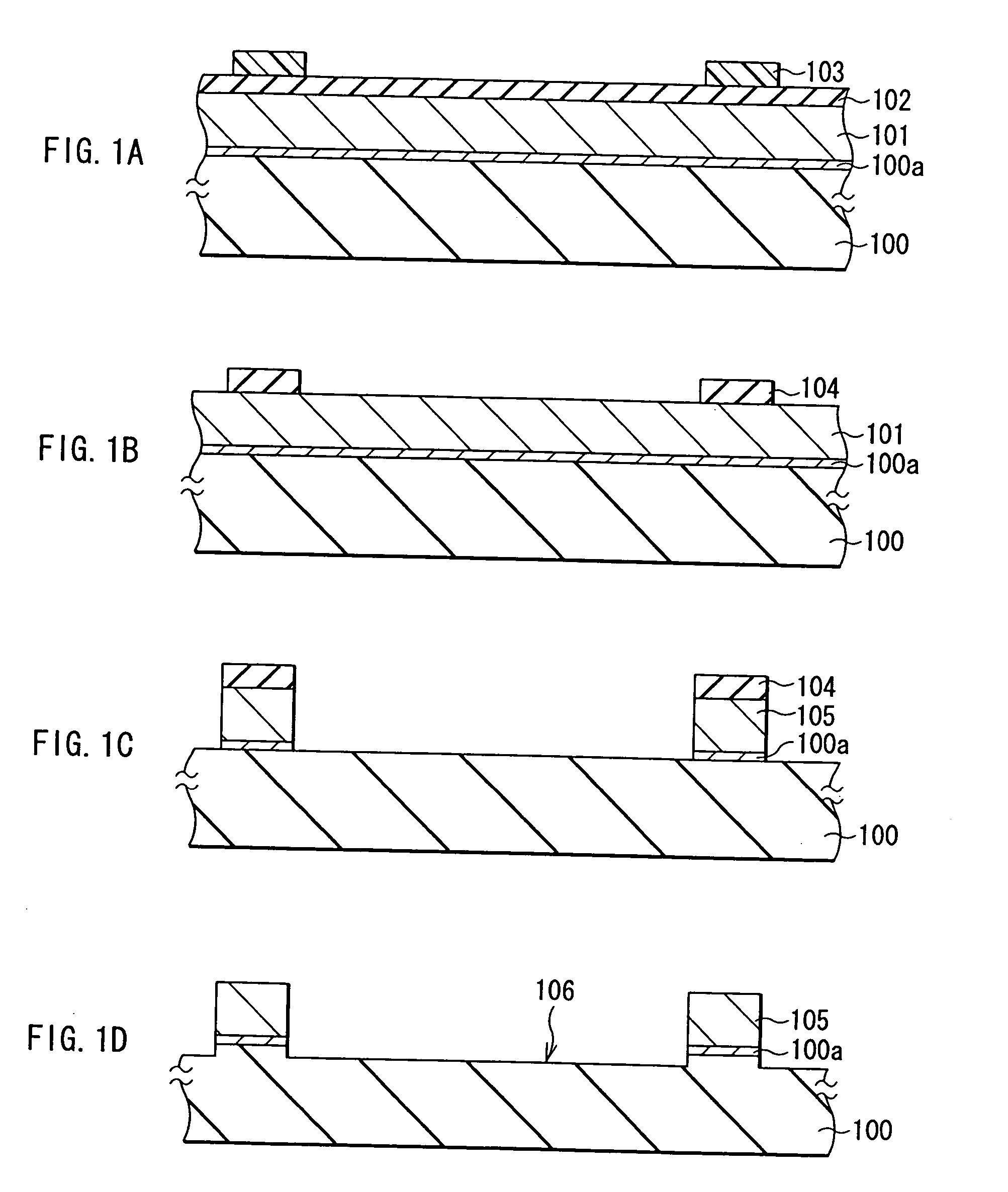
[0040]FIGS. 1A to 5B explain a manufacturing method for a nitride semiconductor according to a first embodiment of the present invention in order. At first, the embodiment will explain the manufacturing method for the nitride semiconductor referring to these Figures. The nitride semiconductor here is a gallium nitride compound containing gallium (Ga) and nitrogen (N), and examples thereof can include GaN, an AlGaN (aluminum gallium nitride) mixed crystal, and an AlGaInN (aluminum gallium indium nitride) mixed crystal. They may contain an n-type impurity consisting of a group IV or VI element such as Si (silicon), Ge (germanium), O (oxygen), or Se (selenium), or a p-type impurity consisting of a group II or IV element such as Mg (magnesium), Zn (zinc), or C (carbon), if needed.

[0041] First, as shown in FIG. 1A, a substrate 100 made of Al2O3 (sapphire) is prepared. Others which can be used as the substrate 100, include Si (silicon), SiC (silicon carbide), GaAs (gallium arsenide), MgA...

examples

[0054] Next, Examples of such a nitride semiconductor layer 107 are concretely shown.

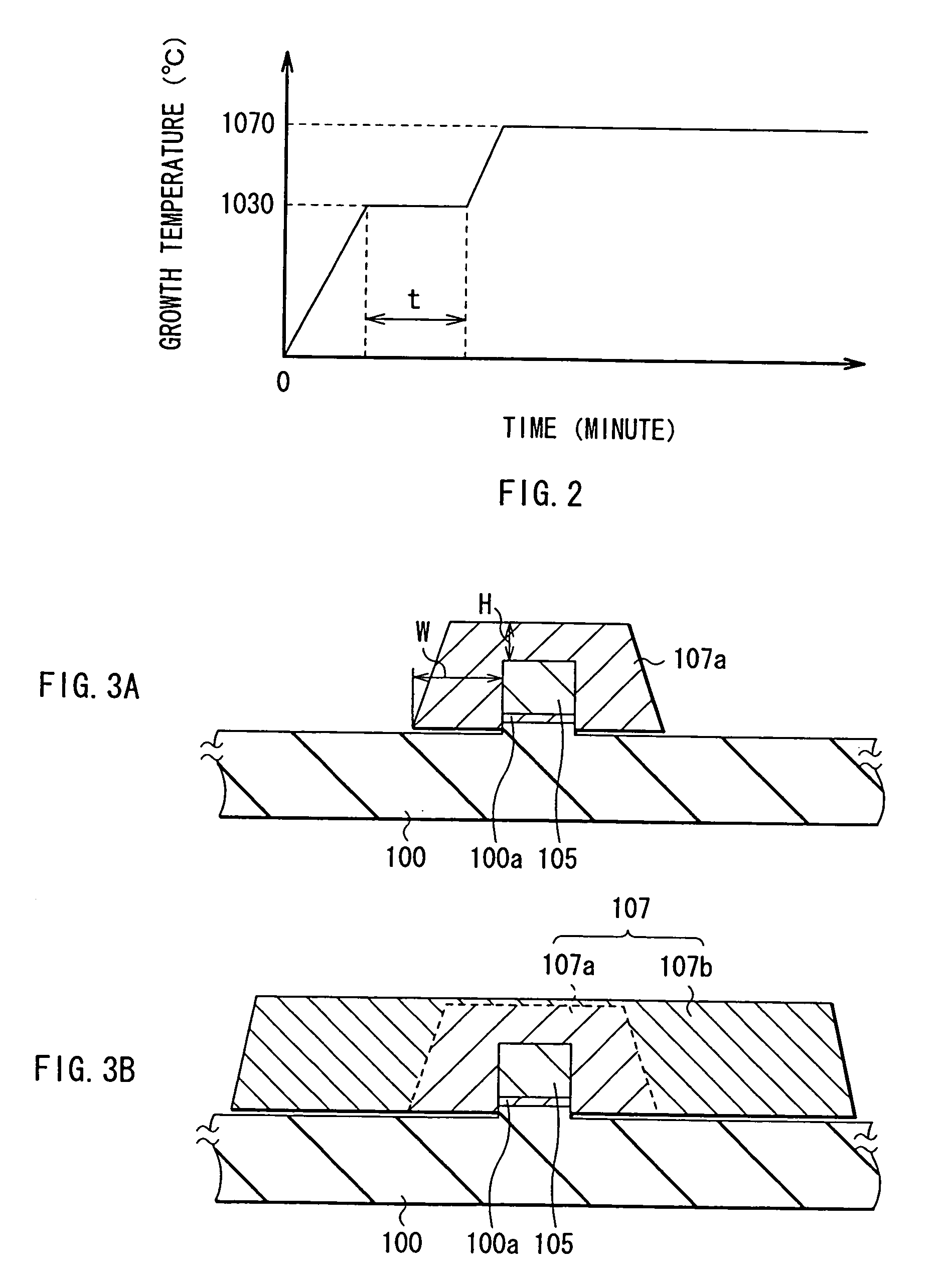
[0055] Like the embodiment, the seed crystal part 105 was formed, and GaN was grown to form the nitride semiconductor layer 107, as the growth temperature was adjusted in accordance with a heat curve in FIG. 2. At that time, the temperature of the first stage was changed from 1030° C. to 1070° C., the temperature of the second stage was fixed to 1070° C., and a hillock density of the formed nitride semiconductor layer 107 was estimated.

[0056]FIG. 6 shows a hillock relative density to the growth temperature in the first stage. As shown in FIG. 6, a generating situation of the hillocks has correlation with the growth temperature of the first stage, and a low temperature region with little hillocks (where a relative ratio of the hillock density is 0) and a high temperature region with many hillocks (where the relative ratio of the hillock density is 1) are observed. Change between two states is not d...

second embodiment

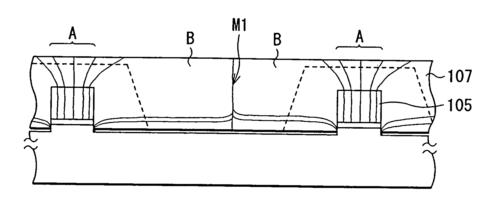
[0072]FIGS. 11A-11C show manufacturing steps of a nitride semiconductor according to a second embodiment in order, and FIGS. 12A-12C show a dislocation situation spreading in a crystal growth process corresponding to the manufacturing steps. A nitride semiconductor layer 207 is formed from the seed crystal parts 105 in the embodiment, and crystal growth is performed in two stages changing a growth temperature. Here, the steps until the seed crystal parts 105 are formed are the same as those of the first embodiment (referring to FIGS. 1A-1D), so the same signs are given to the same components and explanation thereof is omitted.

[0073] The seed crystal parts 105 are pre-formed on the buffer layer 100a which is on the substrate 100, like the first embodiment. The seed crystal parts 105 have a stripe pattern and are separated mutually, for example, and a spreading direction thereof is a direction. First, as shown in FIG. 11A, GaN:Si is grown based on the seed crystal parts 105 to form ...


PUM

PropertyMeasurementUnit
distanceaaaaaaaaaa
widthaaaaaaaaaa
widthaaaaaaaaaa

Abstract

A nitride semiconductor having a large low-defect region in a surface thereof, and a semiconductor device using the same are provided. Also, a manufacturing method for a nitride semiconductor comprising a layer formation step using a transverse growth technique where surface defects can easily be reduced, and a manufacturing method for a semiconductor device using the same are provided. On a substrate, a seed crystal part is formed in a stripe pattern with a buffer layer in between. Next, crystals are grown from the seed crystal part in two stages of growth conditions to form a nitride semiconductor layer. Low temperature growing parts with a trapezoid shaped cross section are formed at a growth temperature of 1030° C. in the first stage and a transverse growth is dominantly advanced at a growth temperature of 1070° C. to form a high temperature growing part between the low temperature growing parts in the second stage. Thereby, hillocks and conventional lattice defects are reduced in a surface of the nitride semiconductor layer which is above the low temperature growing part.

Description

BACKGROUND OF THE INVENTION [0001] 1. Field of the Invention [0002] The present invention relates to a nitride semiconductor, for example, which is used for manufacturing a semiconductor laser device or the like, a semiconductor device using the same, and manufacturing methods for the same. [0003] 2. Description of the Related Art [0004] In recent years, III-V group compound semiconductors attract attention as a device material because of their various characteristics. Especially these materials are direct transition type ones and have a band gap width ranging from 1.9 eV to 6.2 eV, so only these materials provide light emitting in a wide region raging from a visible region to an ultraviolet region, and developments thereof as a material of semiconductor light emitting devices such as a semiconductor laser and light emitting diode (LED) are actively progressing. In addition to their wide band gap width, it can be expected that they have high electron saturation velocity and a high b...

Claims


Application Information

Patent Timeline
Patent Type & Authority Applications(United States)
IPC IPC(8): H01L21/20H01L29/04H01L29/20H01L33/00
CPCH01L29/045H01L29/2003H01L33/007H01L21/02645H01L21/02458H01L21/0254H01L21/0262H01L21/02389H01S5/30
Inventor GOTO, OSAMUASANO, TAKEHARUTAKEYA, MOTONOBUYANASHIMA, KATSUNORIIKEDA, SHINROSHIBUYA, KATSUYOSHISUZUKI, YASUHIKO
Owner SONY CORP
Why Eureka
Try Eureka