

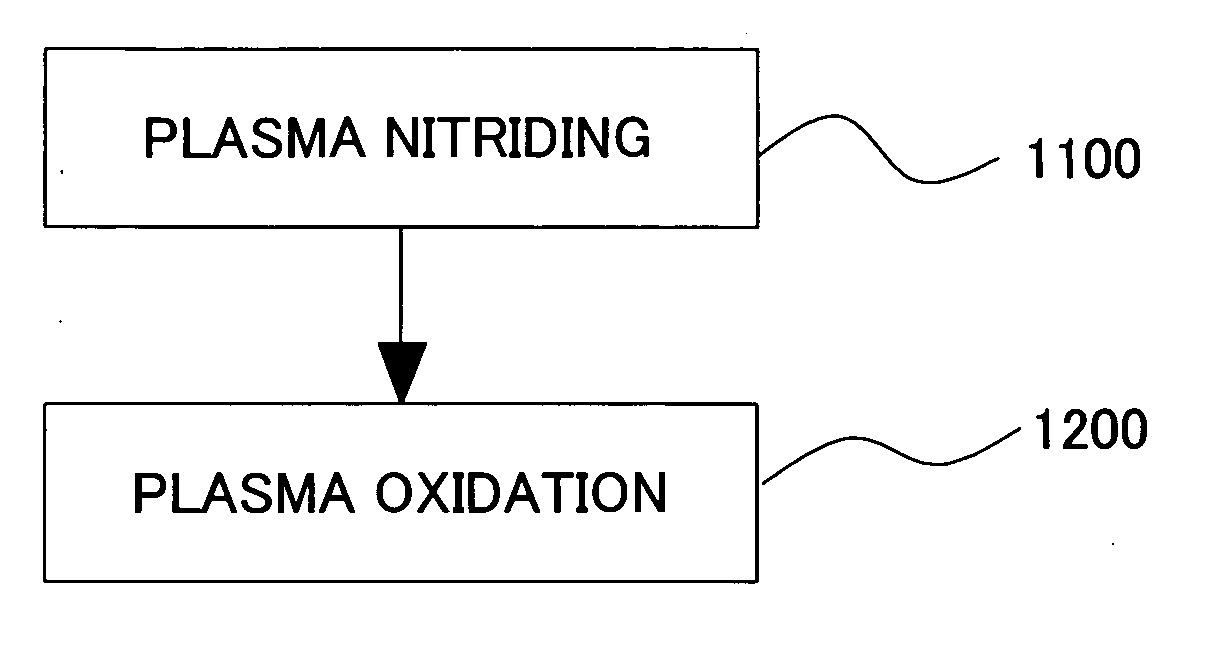
Processing apparatus and method
a processing apparatus and technology of plasma, applied in the direction of mechanical measurement arrangement, vehicle tyre testing, instruments, etc., can solve the problems of preventing fine processing, rediffusion of impurities already present in the substrate, and difficulty in maintaining the performance of a thin film as an insulated film in a thin film region
- Summary
- Abstract
- Description
- Claims
- Application Information
AI Technical Summary
Benefits of technology
Problems solved by technology
Method used
Image

Examples
first embodiment
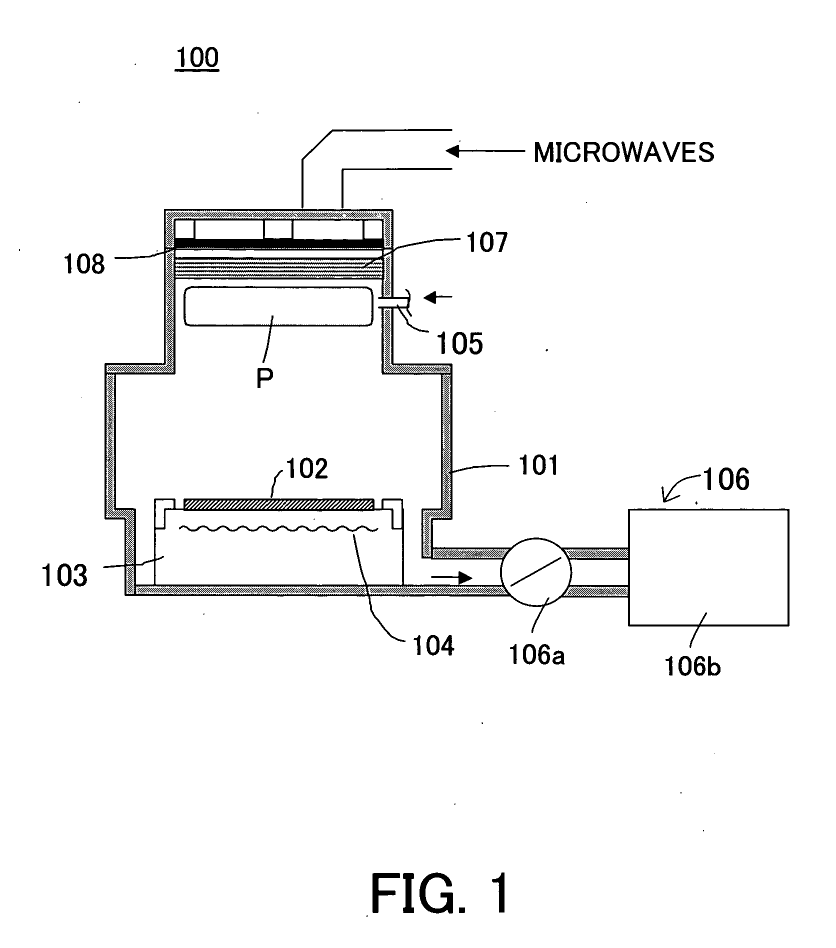
[0049] This embodiment used a microwave plasma processing apparatus 100A shown in FIG. 2 as one example of the processing apparatus 100 to form a gate oxide film for a semiconductor device. The processing apparatus 100A uses the microwaves to excite surface-wave interference plasma, and continuously performs the nitriding and oxidization treatments in the same process chamber. 108A is a slot-cum non-terminal circle waveguide for introducing the microwaves into the plasma processing chamber 101 through the dielectric window 107. Those elements in FIG. 3 which are the same as those in FIG. 1 are designated by the same reference numeral, and which are variations or specific examples of those in FIG. 1 are designated by the same reference numeral with a capital.
[0050] The slot-cum non-terminal circle waveguide 108A has a TE10 mode, a size of an internal wall section of 27 mm×96 mm (with a guide wavelength of 158.8 mm) and a central diameter of the waveguide of 151.6 mm (one peripheral ...
second embodiment
[0056] This embodiment used a microwave plasma processing apparatus 100B shown in FIG. 5 as one example of the processing apparatus 100 to form a gate oxide film for a semiconductor device. The processing apparatus 100B uses a high-frequency power source 110 that can excite plasma in a RF manner and project pulsed power, and performed the nitriding and oxidization treatments. The instant embodiment conducted, as shown in FIG. 8, plasma treatments in the different process chambers 301 and 302 for the nitriding and oxidization treatments. Those elements in FIG. 5 which are the same as those in FIG. 1 are designated by the same reference numeral, and which are variations or specific examples of those in FIG. 1 are designated by the same reference numeral with a capital.
[0057] The substrate 102 used an 8-inch P-type single crystal silicon substrate with a surface azimuth of and resistivity of 10 Ωcm. First, the substrate 102 was fed to the plasma process chamber 101 and placed on the ...
third embodiment
[0061] The third embodiment used different plasma excitation means for the nitriding and oxidization treatments. First, this embodiment formed a silicon nitride film using the processing apparatus 100A for the nitriding treatment.
[0062] The substrate 102 used an 8-inch P-type single crystal silicon substrate with a surface azimuth of and resistivity of 10 Ωcm. First, the substrate 102 was fed to the plasma process chamber 101 and placed on the susceptor 103. The heater 104 heated the substrate 102 up to 400° C. and maintained the temperature.
[0063] Then, mixed gas of N2 and He was introduced at flow rates of 50 sccm and 450 sccm, respectively, into the plasma process chamber 101 to adjust an opening of the pressure control valve 106a, and to hold the pressure in the process chamber 101 to be 26.6 Pa. Then, the microwave supply unit 108A supplied 1 kW microwave power at 2.45 GHz to the process chamber 101 through the dielectric window 107, and generated plasma P in the process cha...
PUM
| Property | Measurement | Unit |
|---|---|---|
| temperature | aaaaa | aaaaa |
| thickness | aaaaa | aaaaa |
| ion energy | aaaaa | aaaaa |
Abstract
Description
Claims
Application Information