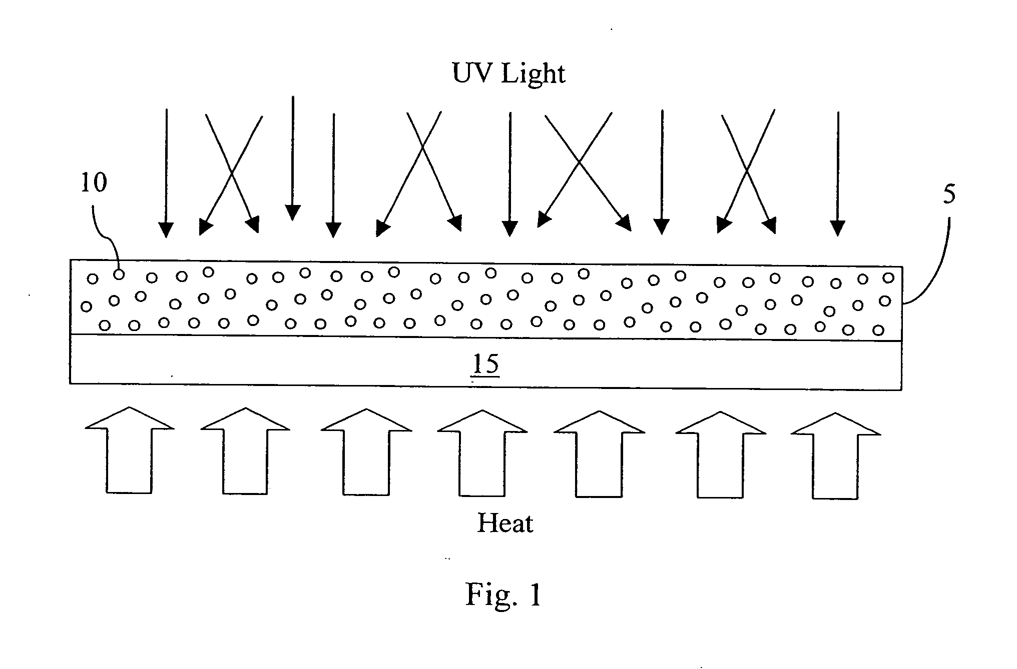
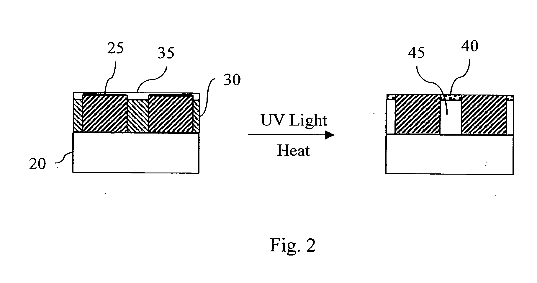

Porous materials

a technology of porous materials and materials, applied in the field of porous materials, can solve the problems of increasing the number of process steps required, not having sufficient mechanical strength to withstand the forces and stresses used in the manufacture of semiconductor devices, and achieving the effects of improving mechanical properties, improving electrical properties, and improving mechanical properties

Inactive Publication Date: 2005-05-26
ROHM & HAAS ELECTRONICS MATERIALS LLC
View PDF19 Cites 36 Cited by
  • Summary
  • Abstract
  • Description
  • Claims
  • Application Information

AI Technical Summary

Benefits of technology

[0052] An advantage of the present invention is that porous organic polysilica films are produced that have better mechanical properties (i.e. higher modulus values) and better electrical properties (i.e. lower dielectric constant) compared to porous organic polysilica material prepared by conventional curing techniques. Also, the carbon residue content in the present organic polysilica films is reduced as compared to the same films prepared by conventional furnace heat curing. Such porous organic polysilica films are also prepared in fewer steps than conventional porous organic polysilica films.
[0053] Further, the present invention provides for porous organic polysilica films having a crack propagation rate of ≦3×10⁻¹⁰ and typically having a thickness of ≧2 μm. More typically, such organic polysilica films have a thickness of ≧2.1 μm, and more typically ≧2.25 μm. In particular, such organic polysilica films have a crack propagation rate of ≦2.9×10⁻¹⁰, and more typically ≦2.5×10⁻¹.
[0054] In another embodiment, the present invention can be used to prepare electronic devices containing more than one porous organic polysilica layer. For example, a first organic polysilica composition containing a first porogen may be disposed on a substrate and optionally dried. A second organic polysilica composition containing a second porogen may then be disposed on the first organic polysilica composition and optionally dried. The first and second organic polysilica compositions may be the same or different. Likewise, the first and second porogens may be the same or different. The multilayer organic polysilica device may then be processed according to the present invention to provide a first porous organic polysilica film and a second porous organic polysilica disposed on the first porous organic polysilica film. The first and second porogens may be chosen so that they are removed at the same time or the second porogen can be at least partially removed before the first porogen. It will be appreciated that more than two porogen containing organic polysilica layers may be used.
[0055] In a further embodiment, the composition containing an organic polysilica partial condensate and a porogen may be disposed on a removable material, such as an air gap forming material. The composition may then be optionally dried. The organic polysilica partial condensate may the be processed according to the present invention. The combination of UV light having a wavelength of ≧190 nm and heating the organic polysilica film to a temperature of 250° to 425° C. forms a porous organic polysilica film and may also remove the removable material to form an air gap structure. In this procedure, an air gap structure is formed under a porous organic polysilica layer. FIG. 2 illustrates a cross-sectional view of a step in the manufacture of an integrated circuit having an air gap structure. In FIG. 2, lines 25 are disposed on substrate 20. Removable material (i.e., air gap forming material) 30 is disposed on substrate 20 and between lines 25. A composition containing an organic polysilica partial condensate and porogen are disposed over lines 25 and removable material 30. The device is then exposed to UV light having a wavelength of ≧190 nm and heating the organic polysilica film to a temperature of 250° to 425° C. to form a device having air gaps 45 under porous organic polysilica layer 40. Accordingly, the present invention can be used to form porous organic polysilica layers and air gap layers in a single processing step.
[0056] The following examples are expected to further illustrate various aspects of the present invention, but are not intended to limit the scope of the invention in any aspect. General Experimental Procedures
[0057] The following general procedures are used in the following Examples.

Problems solved by technology

A disadvantage of certain dielectric materials, including organic polysilica dielectric materials, is that they may not have sufficient mechanical strength to withstand the forces and stresses used in the manufacture of a semiconductor device including the steps of chemical mechanical planarization (“CMP”), wire bonding, wafer dicing, ball bonding, solder reflow and packaging.
This method increases the number of process steps required during the manufacture of a semiconductor device.

Method used


Image

  • Porous materials
  • Porous materials
  • Porous materials

Examples


example 1

[0063] A 1 L 3-neck round bottom flask equipped with a thermometer, condenser, nitrogen inlet, and magnetic stirrer was charged with 120 g of propylene glycol methyl ether acetate (“PGMEA”), 41.8 g of deionized (“DI”) H20, 40 g of EtOH, and 0.56 g of 0.0959 N HCl water solution. After stirring for 5 min., 64.0 g (0.36 mol) of methyl triethoxysilane (“MTES”) and 64.0 g (0.31 mol) of tetraethoxysilane (“TEOS”) were mixed and charged to the flask. The catalyst concentration was about 8 ppm. The cloudy mixture became clear in 30 min. and was stirred for additional 30 min. Then it was heated to 78° C. and held at 78°- 82° C. for 1 hr. After cooling to room temperature, the reaction mixture was charged 10:1 on a weight basis (partial condensate solution to ion exchange resin) with conditioned IRA-67 ion exchange resin in a NALGENE™ high density polyethylene (“HDPE”) bottle. The resulting slurry was agitated using a roller for 1 hr. The IRA-67 resin was removed by filtration. 80g of PGMEA ...

example 2

[0065] A porogen polymer particle solution including as polymerized units 90 wt % methoxypolypropyleneglycol(260) acrylate cross-linked with 10 wt % trimethylolpropane trimethacrylate in propylene glycol methyl ether acetate was prepared according to the procedure disclosed in U.S. Pat. No. 6,420,441.

example 3

[0066] Composite solution samples were prepared by combining the solutions described in Examples 1 and 2 at the varying ratio shown in Table 2 on a dry weight basis. Thus, 84 parts on a dry weight basis of SSQ partial condensate prepared by the procedure of Example 1 and 16 parts on a dry weight basis of the porogen polymer particles prepared by the procedure of Example 2 were combined to provide Sample 1. The Comparative Sample contained only SSQ partial condensate and no porogen polymer. Sufficient solvent was added to achieve a final solids level of 20% or less. The solution was then passed through an ion-exchanged comprised of a mixed bed resin comprising AMBERLITE™ IRA-67 anion resin and IRC-748 chelating cation exchange resin (both resins available from Rohm and Haas Company). The solution was then filtered using a 0.1 μm filter. Finally, the solution was stabilized by the addition of a 100 ppm malonic acid based on the weight of SSQ partial condensate.

[0067] A portion of eac...


PUM

PropertyMeasurementUnit
temperatureaaaaaaaaaa
thicknessaaaaaaaaaa
mole ratiosaaaaaaaaaa

Abstract

Methods of manufacturing a porous organic polysilica dielectric film are provided, such method using a combination of UV and thermal energy. These methods both cure the organic polysilica dielectric material and remove the porogen.

Description

BACKGROUND OF THE INVENTION [0001] The present invention relates generally to the field of manufacture of electronic devices. In particular, the present invention relates to the manufacture of integrated circuits containing low dielectric constant material. [0002] As electronic devices become smaller, there is a continuing desire in the electronics industry to increase the circuit density in electronic components, e.g., integrated circuits, circuit boards, multichip modules, chip test devices, and the like without degrading electrical performance, e.g., crosstalk or capacitive coupling, and also to increase the speed of signal propagation in these components. One method of accomplishing these goals is to reduce the dielectric constant of the interlayer, or intermetal, insulating material used in the components. [0003] A variety of organic and inorganic porous dielectric materials are known in the art in the manufacture of electronic devices, particularly integrated circuits. Suitabl...

Claims


Application Information

Patent Timeline
Patent Type & Authority Applications(United States)
IPC IPC(8): C08J9/26C08G77/18C08J9/00H01L21/312H01L21/316H01L21/768H01L23/14
CPCH01L21/02126H01L21/02203H01L21/02216H01L21/02282H01L21/76825H01L21/3122H01L21/31695H01L21/7682H01L21/02348H01L2221/1047
Inventor FILLMORE, WARD G.GALLAGHER, MICHAEL K.ADAMS, TIMOTHY G.
Owner ROHM & HAAS ELECTRONICS MATERIALS LLC
Features
  • Generate Ideas
  • Intellectual Property
  • Life Sciences
  • Materials
  • Tech Scout
  • Unparalleled Data Quality
  • Higher Quality Content
  • 60% Fewer Hallucinations
Learn More