Method and apparatus for growing silicon carbide crystals

Inactive Publication Date: 2005-06-09
KORDINA OLLE CLAES ERIK +1
View PDF9 Cites 8 Cited by
  • Summary
  • Abstract
  • Description
  • Claims
  • Application Information

AI Technical Summary

Benefits of technology

[0030] Accordingly, an object of the present invention is to provide a method and apparatus for the controlled, extended and repeatable growth of high quality silicon carbide crystals of a desired polytype.
[0031] A further object of the present invention is to provide a method of growing high quality single crystals of silicon carbide by controlling the stoichiometry of the crystal growth process.
[0032] A further object of the present invention is to provide a method of growing high quality single crystals of silicon carbide by controlling the temperature of the crystal growth process.
[0033] A further object of the present invention is to provide a method and apparatus for growing high quality single crystals of silicon carbide by reducing or eliminating impurities resulting from degradation of the physical components of the system.
[0036] A suitable flow of a vaporized species containing silicon and carbon derived from the source of silicon and the source of carbon is generated and maintained within the crucible. The flow of vapor is directed to the growth surface of the seed crystal for a time sufficient to produce a desired amount of macroscopic growth of monocrystalline SiC while substantially preventing any silicon containing species from reacting with material utilized in constructing the SiC crystal growth system.

Problems solved by technology

If the impurities cannot be controlled, the material is generally unsatisfactory for use in electrical devices.
Even in a pure material, a defective lattice structure can prevent the material from being useful.
Addamiano, U.S. Pat. No. 4,556,436 (“Addamiano '436”) discusses a Lely-type furnace system for forming thin films of beta silicon carbide on alpha silicon carbide which is characterized by a rapid cooling from sublimation temperatures of between 2300° C. and 2700° C. to another temperature of less than 1800° C. Addamiano '436 notes that large single crystals of cubic (beta) silicon carbide are simply not available and that growth of silicon carbide or other materials such as silicon or diamond is rather difficult.
75-mm diameter wafers of good quality have been demonstrated but are not yet commercially available and there is already a need for 100-mm wafers.
Many SiC crystal production techniques are simply incapable of economically and consistently producing crystals of the size and quality needed.
The chemistry of silicon carbide sublimation and crystallization is such that the known methods of growing silicon carbide crystals are difficult, even when carried out successfully.
The stoichiometry of the crystal growth process is critical and complicated.
Too much or too little silicon or carbon in the sublimed vapor may result in a crystal having an undesired polytype or imperfections such as micropipes.
Likewise, the high operating temperatures, typically above 2100° C. and the necessity of forming specific temperature gradients within the crystal growth system pose significant operational difficulties.
Therefore, the infrared radiation emitted by the graphite containers can overheat the seed crystal thereby complicating the precise temperature gradients necessary for successful operation of sublimation systems.
The solid carbon source material may also be replaced by a gas such as propane; however, most of the carbon utilized in this technique actually comes from the graphite walls of the crucible.
Unfortunately, the HTCVD technique has not proven commercially useful for boule growth primarily because the reaction destroys the graphite crucibles used in the process.
Furthermore, the addition of hydrocarbon gases in this particular process tends to produce Si droplets encrusted with SiC which decreases efficiency and also ties up Si and C thereby altering the stoichiometry of the system.
Perhaps the most difficult aspect of silicon carbide growth is the reactivity of silicon at high temperatures.
This reaction is difficult to control and usually results in too much silicon or too much carbon being present in the system thus undesirably altering the stoichiometry of the crystal growth process.
In addition, silicon's attack on the graphite container pits the walls of the container destroying the container and forming carbon dust which contaminates the crystal.
The cost of tantalum is, however, a drawback to a sublimation process utilizing the container described in Vodakov.
A sublimation container of solid tantalum is extremely expensive and like all sublimation containers, will eventually fail, making its long-term use un-economic.
A solid tantalum sublimation container is also difficult to machine.
Physically forming such a container is not an easy task.
Lastly, the sublimation process of Vodakov '350 suffers the same deficiency shown in other solid source sublimation techniques in that it is not efficient at forming the large, high quality boules needed for newly discovered applications.

Method used


Image

  • Method and apparatus for growing silicon carbide crystals
  • Method and apparatus for growing silicon carbide crystals
  • Method and apparatus for growing silicon carbide crystals

Examples


Embodiment Construction

[0040] As will be readily apparent to those skilled in the art, the following disclosure may be easily adapted and incorporated into virtually all known methods for producing SiC crystals. Accordingly, the following detailed description will begin with a general discussion of the invention. Additional embodiments demonstrating the versatility of the invention will follow.

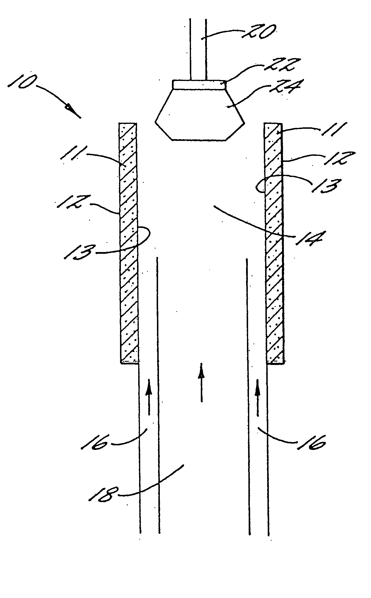
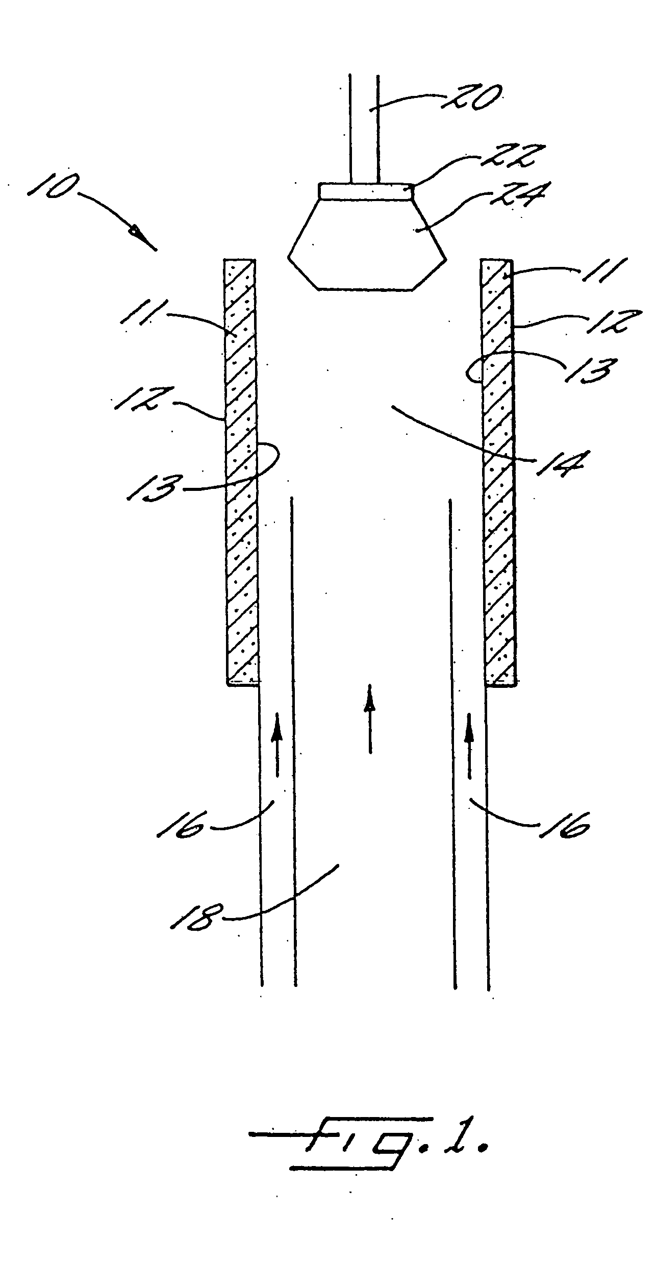
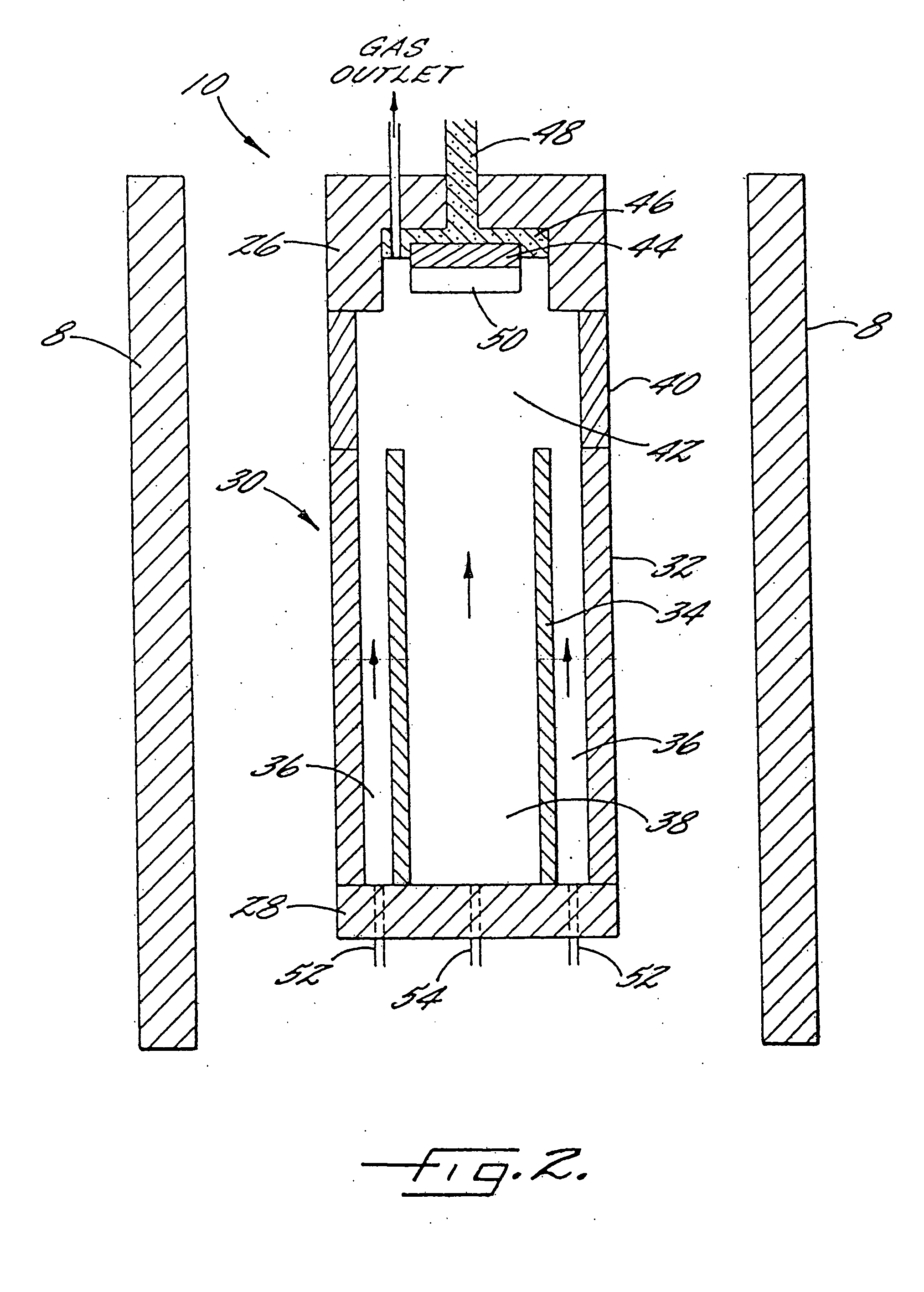
[0041] A preferred embodiment of the invention is a gas fed sublimation (GFS) system in which the source of silicon and the source of carbon are gaseous. The gaseous silicon and carbon sources are fed to a reaction chamber where they react at high temperatures, typically above 2000° C., to form vaporized species containing silicon and carbon. In addition to carbon (C) and silicon (Si), such species typically include SiC, Si2C, and SiC2 The vaporized species are then deposited onto a monocrystalline seed crystal of a desired polytype. Such a system is schematically disclosed in FIG. 1.

[0042] The GFS system of FIG. ...


PUM


Abstract

A method and apparatus for controlled, extended and repeatable growth of high quality silicon carbide boules of a desired polytype is disclosed which utilizes graphite crucibles coated with a thin coating of a metal carbide and in particular carbides selected from the group consisting of tantalum carbide, hafnium carbide, niobium carbide, titanium carbide, zirconium carbide, tungsten carbide and vanadium carbide.

Description

CROSS-REFERENCE TO PRIOR APPLICATIONS [0001] This application is a divisional of application Ser. No. 09 / 415,402 filed Oct. 8, 1999 entitled “Method and Apparatus for Growing Silicon Carbide Crystals.”FIELD OF THE INVENTION [0002] The present invention relates to the high temperature growth of large single crystals, and in particular relates to methods and apparatus for the growth of high-quality single crystals of silicon carbide. BACKGROUND [0003] Silicon carbide is a perennial candidate for use as a semiconductor material. Silicon carbide has a wide bandgap, a low dielectric constant, and is stable at temperatures far higher than temperatures at which other semiconductor materials, such as silicon, become unstable. These and other characteristics give silicon carbide excellent semiconducting properties. Electronic devices made from silicon carbide can be expected to perform, inter alia, at higher temperatures, faster speeds and at higher radiation densities, than devices made fro...

Claims


Application Information

Patent Timeline
IPC IPC(8): C30B23/00C30B25/00C30B29/36
CPCC30B23/00C30B25/00Y10S117/90Y10S117/902C30B29/36
Inventor KORDINA, OLLE CLAES ERIKPAISLEY, MICHAEL JAMES
Owner KORDINA OLLE CLAES ERIK
Why Eureka
Try Eureka