Semiconductor device and manufacturing method thereof

a semiconductor and semiconductor technology, applied in semiconductors, solid-state devices, capacitors, etc., can solve the problems of increasing coupling capacitance, mim capacitors, difficult to build passive devices into ic chips, etc., to reduce dielectric breakdown strength, reduce leakage current, and enhance the capacitance density of mim capacitors

Inactive Publication Date: 2005-09-29
HITACHI LTD
View PDF5 Cites 58 Cited by
  • Summary
  • Abstract
  • Description
  • Claims
  • Application Information

AI Technical Summary

Benefits of technology

[0027] According to the present invention, it becomes possible, while enhancing the capacitance density of an MIM capacitor and minimizing an increase in leakage current and a decrease in dielectric breakdown strength, to reduce any leaka...

Problems solved by technology

In the past, these passive devices have been difficult to build into IC chips and have therefore been mounted as external components on substrates.
This capacitor, however, has problems including the ones that the use of an electrode material which contains polysilicon increases resistance, and that since the deposition temperature of the polysilicon exceeds the maximum permissible temperature in a wiring process, the capacitor must be formed near a silicon substrate and this also increases coupling capacitance.
The thus-formed MIM capacitor, however, has the disadvantage that it cannot easily enhance performance.
Accordingly, there have been the problems in that it is difficult to reduce the area occupied by MIM elements in one IC chip and thus in that the IC chip itself increases in area.
The thus-formed MIM capacitor,...

Method used


Image

  • Semiconductor device and manufacturing method thereof
  • Semiconductor device and manufacturing method thereof
  • Semiconductor device and manufacturing method thereof

Examples


first embodiment

[0059]FIGS. 7A to 7C and 8A to 8C are sectional views showing a manufacturing process for a semiconductor device based on a first embodiment of the present invention. The description below is given in order of process steps. First, as shown in FIG. 7A, on a substrate 100 having semiconductor devices formed thereon, a first barrier metal film 200 made of 50-nm-thick titanium nitride, a first aluminum film 201 made of a 400-nm-thick aluminum alloy, and a second barrier metal film 202 made of 50-nm-thick titanium nitride are formed using a sputtering method. After this, a first intermediate layer 300 made of a 100-nm-thick silicon dioxide film is formed using a plasma CVD method, and then a first opening 500 is formed in a desired area of the first intermediate layer 300 by using lithography and dry etching. Next, a dielectric film 400 made of 50-nm-thick tantalum oxide, an upper electrode 203 made of 50-nm-thickness titanium nitride, and a hard mask 301 made of 100-nm-thick silicon di...

second embodiment

[0077]FIGS. 12A to 12C, 13A and 13B are sectional views showing another manufacturing process for a semiconductor device of the present invention. The description below is given in order of process steps.

[0078] First, as shown in FIG. 12A, on a substrate 100 having semiconductor devices formed thereon, a first barrier metal film 200 made of 50-nm-thick titanium nitride, a first aluminum film 201 made of a 400-nm-thick aluminum alloy, and a second barrier metal film 202 made of 50-nm-thick titanium nitride are formed using a sputtering method. After this, a first intermediate layer 300 made of a 100-nm thick silicon dioxide film is formed using a plasma CVD method, and then an opening is provided in a desired area of the first intermediate layer 300 by using lithography and dry etching. Next, a dielectric film 400 made of 50-nm-thick tantalum oxide, and an upper electrode 203 made of 50-nm-thick titanium nitride are formed by reactive sputtering and lithography, respectively, in suc...

third embodiment

[0094]FIGS. 14A, 14B15A, and 15B are sectional views showing yet another manufacturing process for a semiconductor device of the present invention. The description below is given in order of process steps.

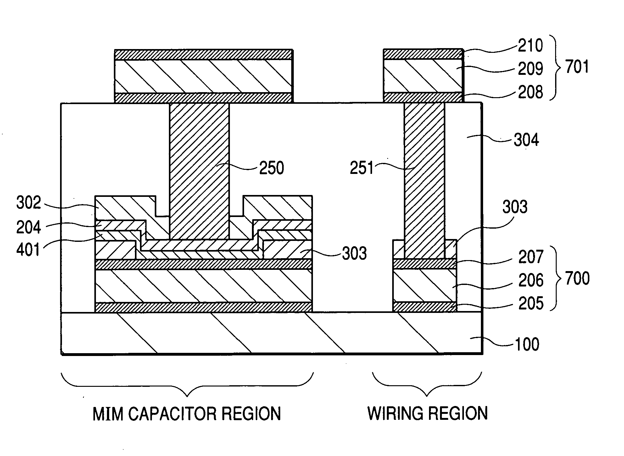
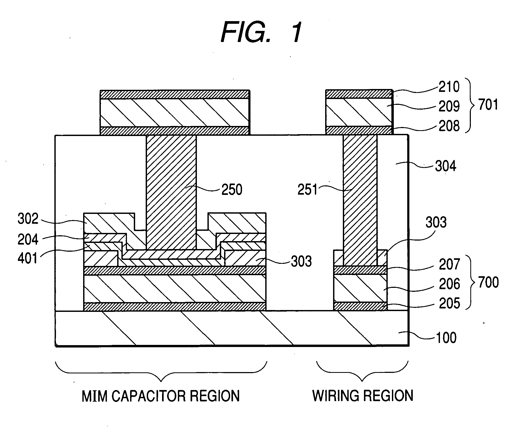
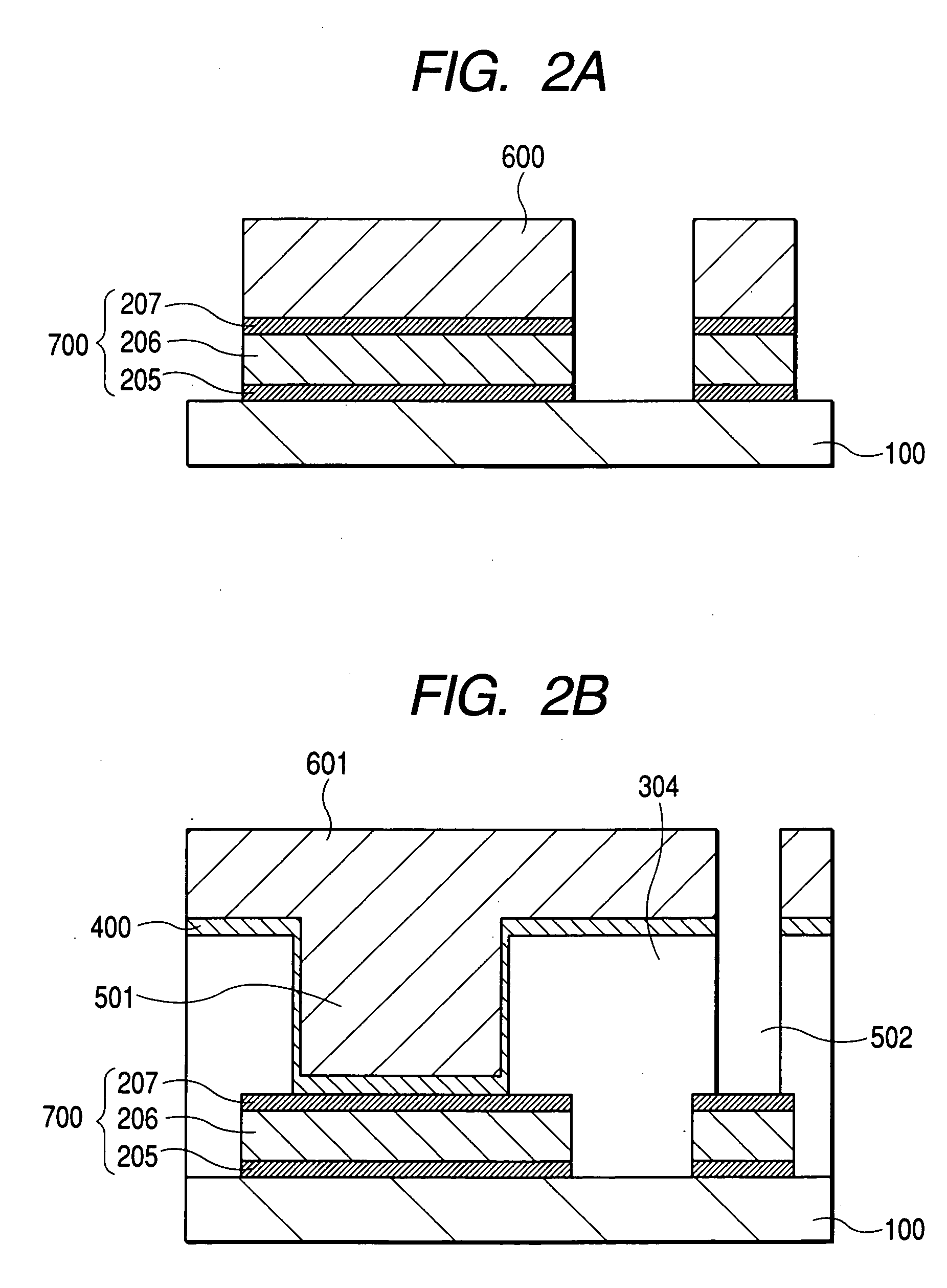
[0095] First, as shown in FIG. 14A, on a substrate 100 having semiconductor devices formed thereon, a titanium nitride film with a film thickness of 50 nm, an aluminum alloy with a film thickness of 400 nm, and another titanium nitride film with a film thickness of 50 nm are formed using a sputtering method. After that, first metal wiring 700 including a first barrier metal layer 205, a first aluminum layer 206, and a second barrier metal layer 207, is formed using lithography and dry etching. Next, a first interlayer dielectric layer 304 made of a 1000-nm-thick silicon dioxide film is formed using plasma CVD, and then the first interlayer dielectric layer 304 is made planar by chemical-mechanical polishing. Next after a desired area of the first metal wiring 700 is exposed by for...


PUM


Abstract

An MIM capacitor using a high-permittivity dielectric film such as tantalum oxide. The MIM capacitor includes an upper electrode, a dielectric film, and a lower electrode. A second dielectric film and the dielectric film are formed between the upper electrode and the lower electrode, at the end of the MIM capacitor. The second dielectric film is formed to have an opening at the top of the lower electrode. The dielectric film abuts the lower electrode via the opening. The upper electrode is formed on the dielectric film. The upper electrode and the dielectric film are formed in such a manner as to embrace the opening entirely, and the second dielectric film and the lower electrode are formed so that the respective widths are the same as, or greater than, the widths of the upper electrode and the dielectric film.

Description

CLAIM OF PRIORITY [0001] The present application claims priority from Japanese application JP2004-091207, filed on Mar. 26, 2004, the contents of which are hereby incorporated by reference into this application. BACKGROUND OF THE INVENTION [0002] 1. Field of the Invention [0003] The present invention relates to a semiconductor device having a high-reliability high-performance capacitor, and to a method of manufacturing the semiconductor device. [0004] 2. Description of the Related Art [0005] In the integrated circuits (ICs) that handle analog signals, capacitors, resistors, inductors, and other passive devices become important constituent elements of the ICs. In the past, these passive devices have been difficult to build into IC chips and have therefore been mounted as external components on substrates. In recent years, however, incorporating the passive devices into IC chips has been attempted actively in order to meet the strong needs of faster system operation and space saving. ...

Claims


Application Information

Patent Timeline
IPC IPC(8): H01L21/02H01L21/768H01L27/108
CPCH01L28/40H01L21/76838
Inventor TAKEDA, KENICHIFUJIWARA, TSUYOSHIIMAI, TOSHINORIISHIKAWA, TSUYOSHIMINE, TOSHIYUKIMIURA, MAKOTO
Owner HITACHI LTD
Why Eureka
Try Eureka