Semiconductor device and manufacture method thereof
- Summary
- Abstract
- Description
- Claims
- Application Information
AI Technical Summary
Benefits of technology
Problems solved by technology
Method used
Image


Examples
embodiment 1
[0032] A method for forming a crystalline silicon film using this invention will be explained in conjunction with FIG. 1.
[0033] Base-material insulating film 101 is formed on substrate 100. As the base-material insulation film 101, a silicon nitride film, a silicon oxide film, a silicon oxynitride film or the like can be used. Incidentally, when using quartz for a substrate, the process to form the base-material insulating film 101 can be skipped.
[0034] Subsequently, amorphous silicon film 102 is formed as a semiconductor film on the base-material insulating film 101. Amorphous silicon film 102 is satisfactorily formed in the film thickness of 50 to 200 nm using well-known CVD method or sputtering method.
[0035] Subsequently, after hydrofluoric acid removes impurities and the natural oxide film adhering to the obtained amorphous silicon film surface so as to be clean, the surface is further processed with ozone water. Then a very thin (1 to 5 nm) oxide film is formed, and the acet...
embodiment 2
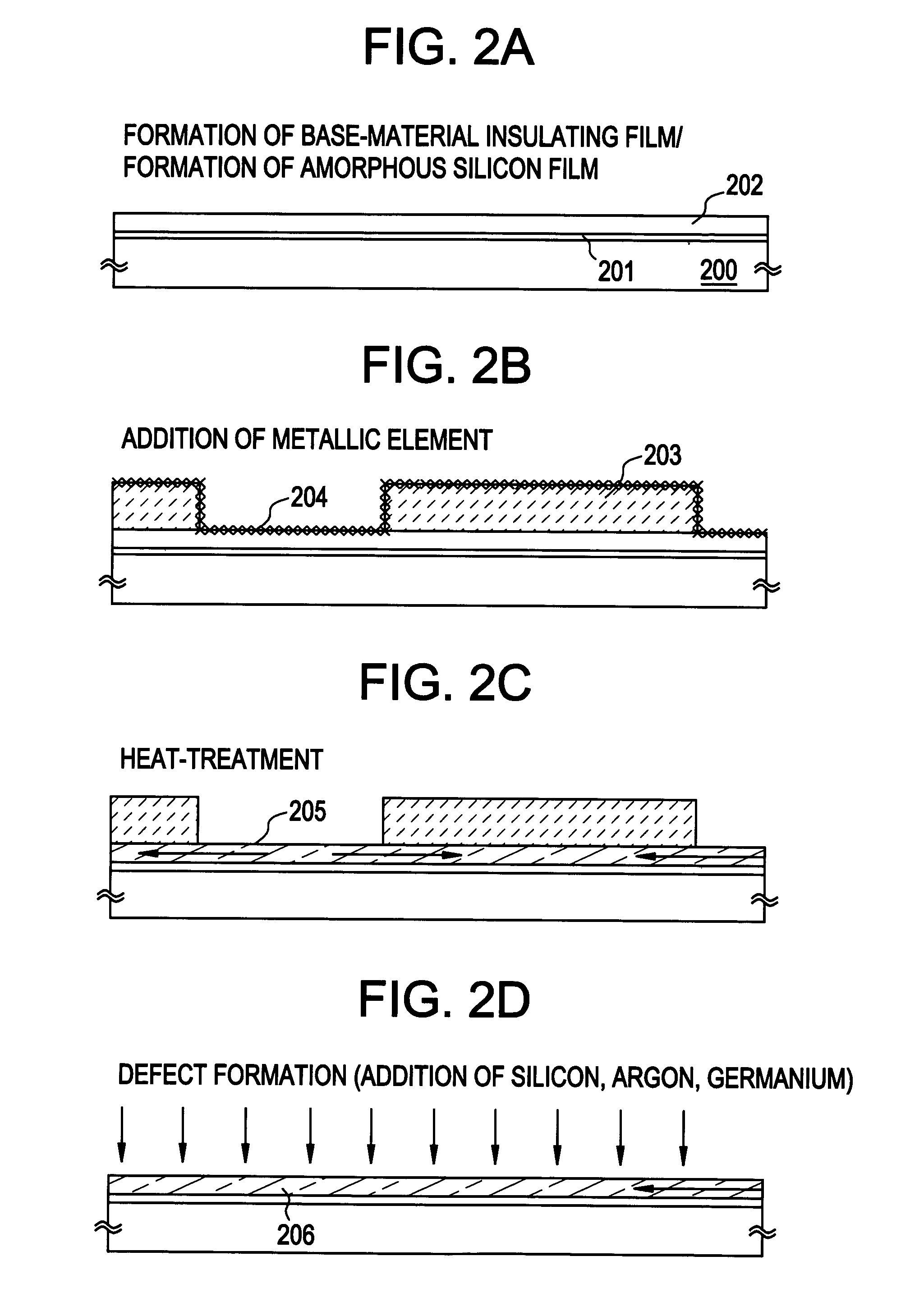
[0040] An example of the manufacture method for a crystalline silicon film, which is different from the embodiment 1, will be explained referring to FIG. 2.
[0041] Base-material insulating film 201 is formed on substrate 200. Either of a silicon nitride film, a silicon oxide film, and a silicon oxynitride film, or laminated films thereof may be applied as base-material insulating films. Incidentally, when using quartz for a substrate, the process of forming the base-material insulating film 201 can be skipped.
[0042] Amorphous silicon film 202 is formed by reduced-pressure CVD method on the base-material insulating film 201. (FIG. 2A). The well known methods such as sputtering method or CVD method is used to form in the film thickness of 50 to 200 nm.
[0043] Next, the surface of the amorphous silicon film 202 is subjected to hydrofluoric acid processing so as to be clean, and silicon oxide is formed by CVD method on the clean silicon film 202. Then an aperture part is formed by etch...
embodiment 3
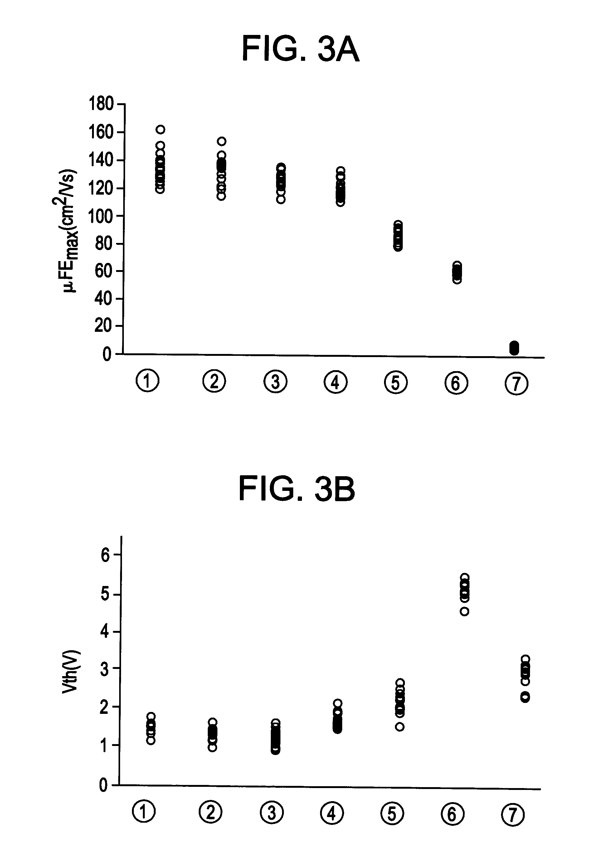
[0050] In this embodiment, TFT which forms a defect by doping argon over a semiconductor layer, and TFT which forms no defects are compared.
[0051] The concentration of the argon doped on the semiconductor film (implanted) is (1) 0 / cm3 (no argon addition) (2) 3.0×10¹⁷ / cm3 (3) 5.0×10¹⁷ / cm3 (4) 2.5×10¹⁸ / cm3 (5) 6.6×10¹⁸ / cm3 (6) 1.4×10¹⁹ / cm3 (7) 3.0×10¹⁹ / cm3. As for each TFT from (1) to (7), the measurement result of a field effect mobility, a threshold value, and OFF current and ON current are shown in FIGS. 3 and 4. Incidentally, the size of a semiconductor layer is channel length L / channel width W=8 / 8 μm.
[0052] First, the field effect mobility value of TFT with argon concentration of (1) to (7) is shown in FIG. 3A. The value of TFT with Argon doping concentration of (2) to (4) is not inferior to TFT of (1) with no argon doped.
[0053] Subsequently, the threshold value of TFT with argon concentration of (1) to (7) is shown in FIG. 3B. TFT with argon doping concentration of (2) to (4)...
PUM
 Abstract
Description
Claims
Application Information
 - Generate Ideas
- Intellectual Property
- Life Sciences
- Materials
- Tech Scout
- Unparalleled Data Quality
- Higher Quality Content
- 60% Fewer Hallucinations
Browse by: Latest US Patents, China's latest patents, Technical Efficacy Thesaurus, Application Domain, Technology Topic, Popular Technical Reports.
© 2025 PatSnap. All rights reserved.Legal|Privacy policy|Modern Slavery Act Transparency Statement|Sitemap|About US| Contact US: help@patsnap.com