

Method of forming a conductive wiring pattern by laser irradiation and a conductive wiring pattern
- Summary
- Abstract
- Description
- Claims
- Application Information
AI Technical Summary
Benefits of technology
Problems solved by technology
Method used
Image

Examples
embodiment 1
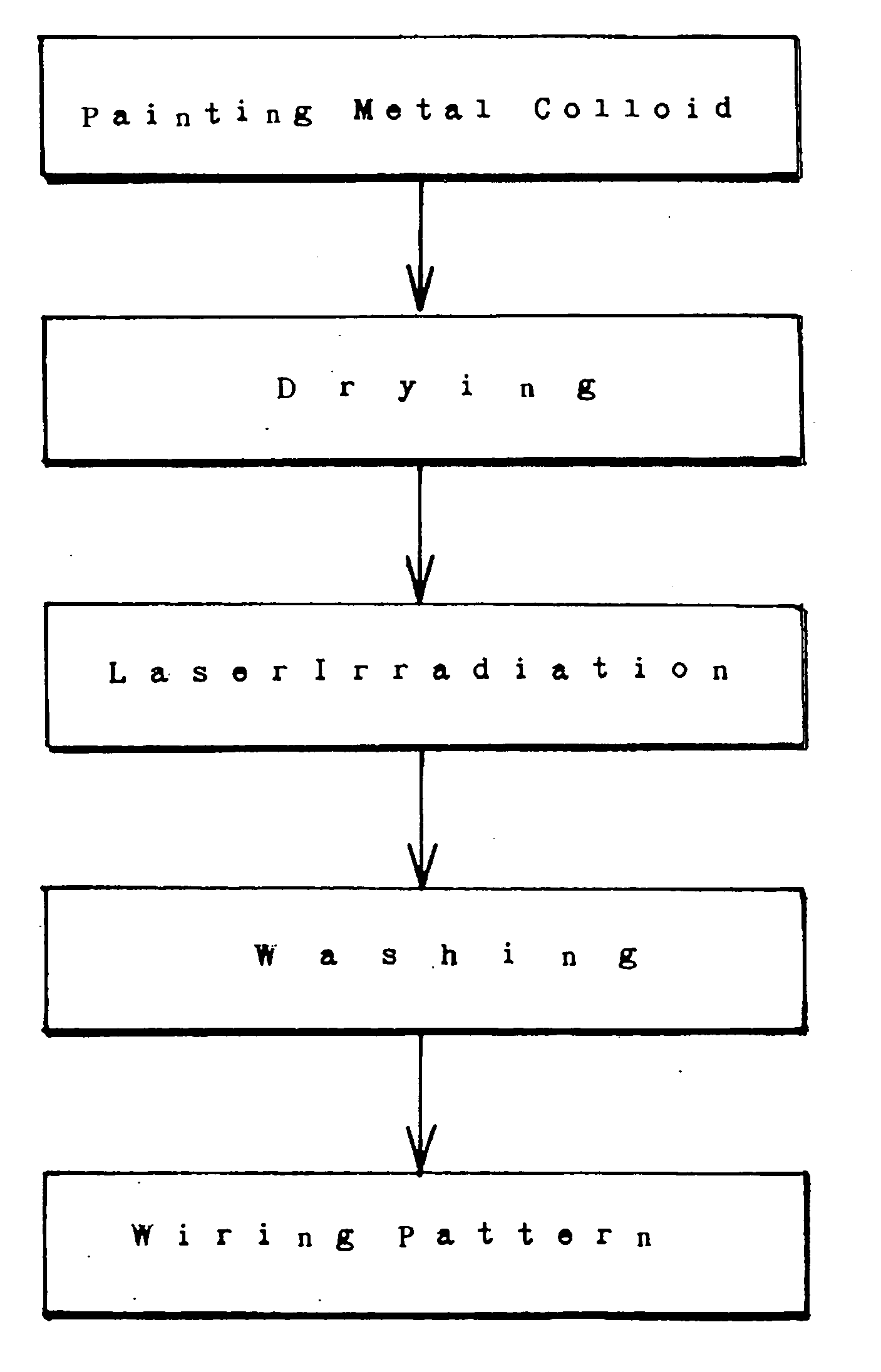
[0121] Polyimide boards, polyethylene terephthalate (PET) boards, glass boards, and ceramic boards are prepared as base boards. The specimen boards are spin-coated with the silver suspension ink as described in the metal suspension colloid 1.
(Spin-Coating)
[0122] A specimen board is vacuum-locked on a disc rotor of a spinner. Metal suspension colloid is dropped on the specimen. The rotor is rotated for thirty seconds at a speed of 200 rpm to 3000 rpm for making a thin suspension colloid film on the specimen board.
(Drying)
[0123] The specimen is dried at 100° C. for 10 minutes. Water (solvent) is fully removed from the metal suspension film. The disperse agent still remains in the metal suspension film. The suspension film has a thickness of about 0.3 μm. The electric resistance is high. The specimen films are insulators. The colloid film is unstable. Washing with water can fully eliminate the suspension film from the specimen board.
[0124] The optical system...
PUM
| Property | Measurement | Unit |
|---|---|---|
| Diameter | aaaaa | aaaaa |
| Diameter | aaaaa | aaaaa |
| Diameter | aaaaa | aaaaa |
Abstract
Description
Claims
Application Information