Ion beam system and machining method

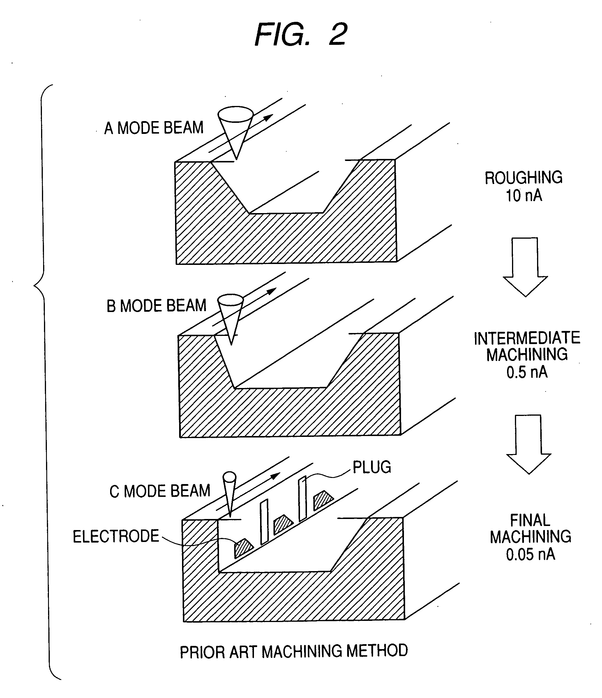
a technology of machining method and beam system, which is applied in the field of machining method, can solve the problems of shortening the time required to prepare an observation/analysis sample from a (larger) sample, and achieve the effects of shortening the time to separate or prepare separation, improving the machining precision of forming a cross-section, and shortening the time to separa

Inactive Publication Date: 2006-03-30
HITACHI HIGH-TECH CORP
View PDF2 Cites 45 Cited by
  • Summary
  • Abstract
  • Description
  • Claims
  • Application Information

AI Technical Summary

Benefits of technology

[0014] In the defect analysis of electronic components, such as semiconductor memories and microprocessors, it is strongly desired to perform plural analyses simultaneously and feedback the analysis results in a short time. Specifically, it is important from the viewpoint of reducing manufacturing cost to extract and prepare an analysis sample as early as possible from a discovered faulty point, to conduct inspection and analysis, and to promptly feed back the obtained results to the manufacturing process. At present, about 5 to 10 minutes is required to form a cross-section by an ion beam, and about 30 to 60 minutes is required to extract a micro sample by an ion beam, but this is not short enough for production line requirements, and shortening of the time required to prepare an observation / analysis sample from a (larger) sample is a current problem.
[0019] It is therefore an object of the present application, which was conceived in view of the aforesaid problem, to improve the yield of a semiconductor device or the like by providing a machining method which can improve the machining precision of forming a cross-section by an ion beam without lengthening the machining time, by providing a machining method which shortens the time to separate or prepare separation of a micro sample without splitting a wafer, and by providing an ion beam system. It is a further object to provide a machining method which shortens the cross-section forming time, to provide a machining method which shortens the time to separate or prepare separation of an analysis sample from a wafer, and to provide an ion beam system when an inert gas, oxygen or nitrogen ions are used for the ion beam.
[0020] In the accordance with present invention, in order to improve machining precision while maintaining the machining time, the beam cross-section of the ion beam is formed in an elliptical shape. By forming it in an elliptical shape, an ion beam having respectively two different diameters in the minor axis and major axis direction of the ellipse can be generated. To machine a sample cross-section, the minor axis direction of a beam spot with a small diameter is used. Thereby, the sample machining precision can be improved as compared with the case where a circular beam is used.
[0025] According to the present application, therefore, there is provided a machining method which can improve the machining precision of forming a cross-section by an ion beam without lengthening the machining time, a machining method which shortens the time to separate or prepare separation of a micro sample without splitting a wafer and an ion beam system. Further provided are a machining method which shortens the cross-section forming time, a machining method which shortens the time to separate or prepare separation of an analysis sample from a wafer and an ion beam system, when an inert gas, oxygen or nitrogen ions are used for the ion beam. Also provided is a novel inspection / analysis method which does not require wafers to be discarded due to testing, and does not generate defects even if wafers from which samples were removed for inspection are returned to the process. By using the electronic component manufacturing method according to the present application, wafers can be tested without splitting the wafer, new defects are not created and expensive wafers are not rendered useless. As a result, the manufacturing yield of electronic component production improves. Finally, there is provided an ion beam system which can implement the method of separating or preparing separation of analysis samples, the inspection / analysis method, and the electronic component manufacturing method.

Problems solved by technology

At present, about 5 to 10 minutes is required to form a cross-section by an ion beam, and about 30 to 60 minutes is required to extract a micro sample by an ion beam, but this is not short enough for production line requirements, and shortening of the time required to prepare an observation / analysis sample from a (larger) sample is a current problem.

Method used


Image

  • Ion beam system and machining method
  • Ion beam system and machining method
  • Ion beam system and machining method

Examples


first embodiment

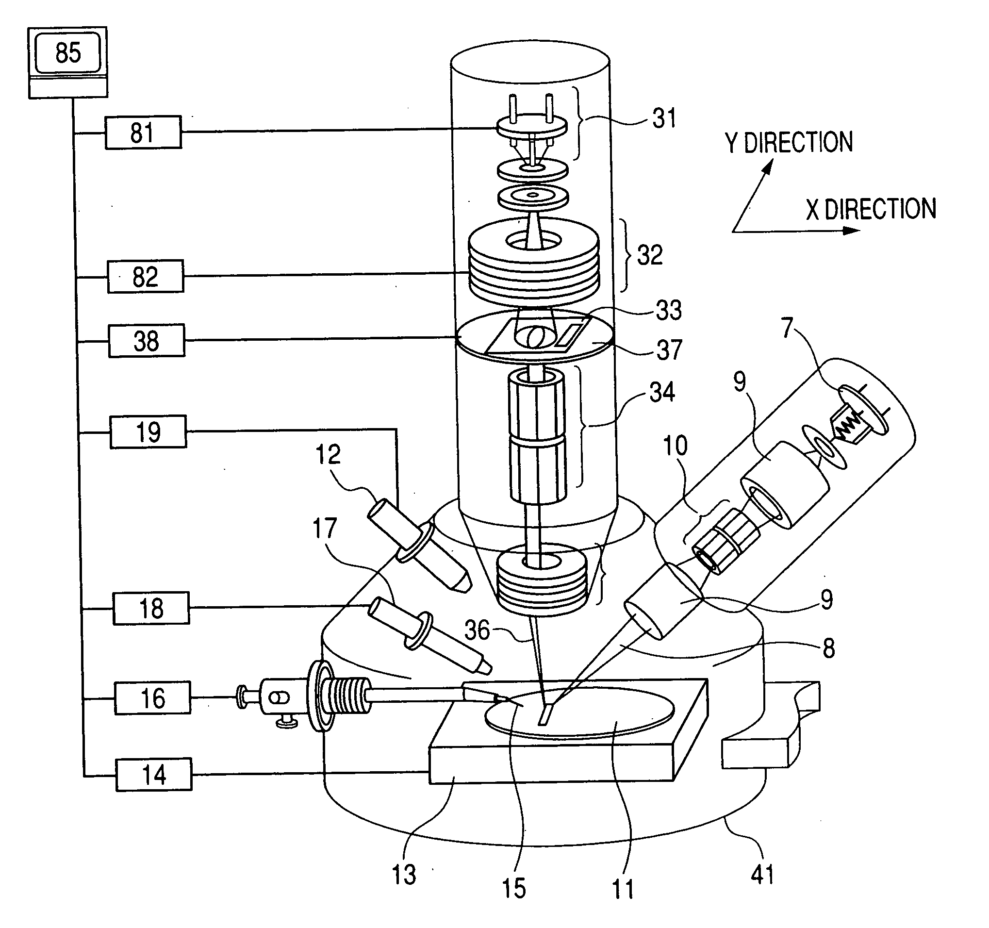
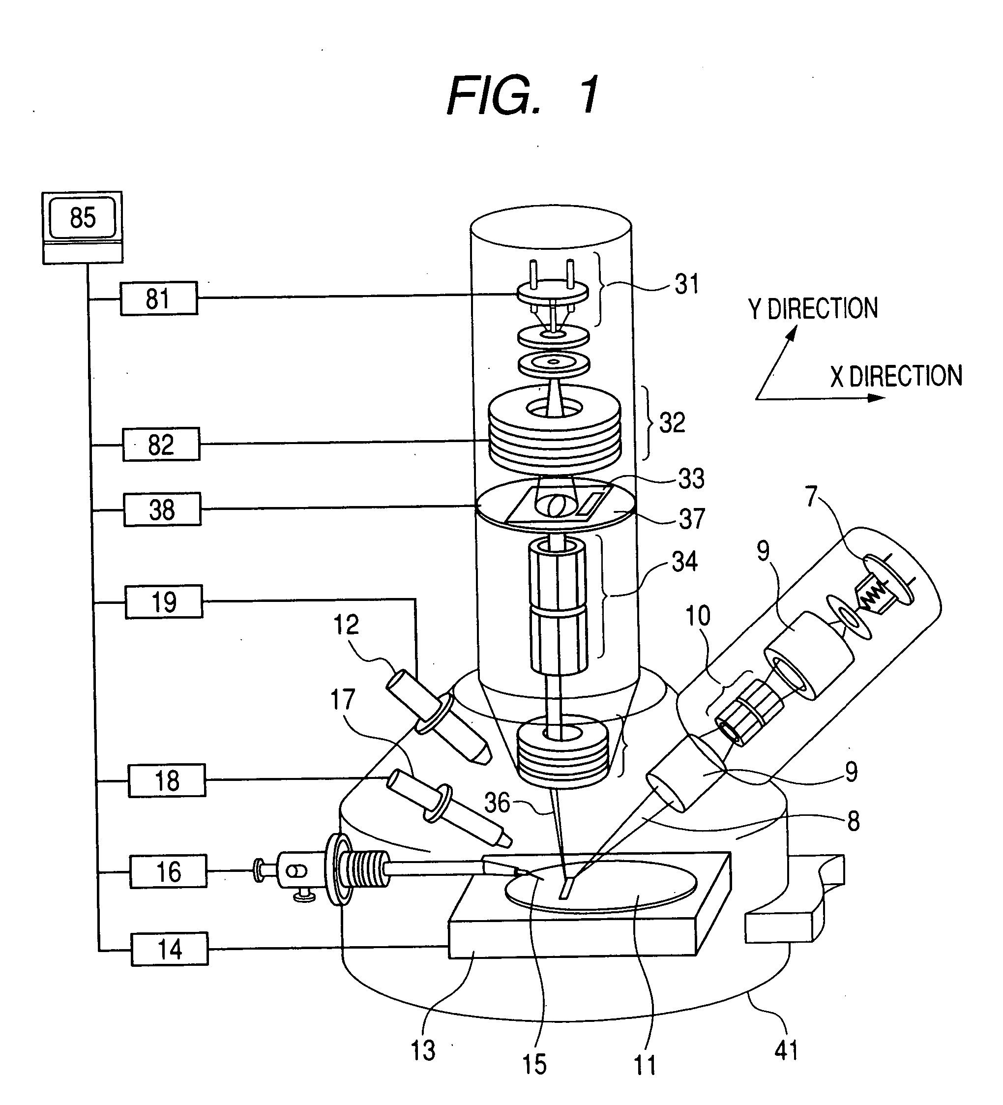
[0048] In this embodiment, an example will be described wherein the shape of the ion beam spot is formed by an aperture having an elliptical or rectangular opening. FIG. 1 is a schematic view of an ion beam system according to this embodiment. This ion beam system 23 comprises a vacuum chamber 41, this vacuum chamber containing an ion beam irradiation system comprising a liquid metal ion source 31 which emits gallium ions, condenser lens 32, beam limiting aperture 33, aperture rotating mechanism 37, ion beam scanning deflector 34 and objective lens 35. An electron beam irradiation system comprising an electron source 7, electron lens 9 which converges the electron beam 8 emitted from the electron source 7 and electron beam scanning deflector 10 are also provided therein. Further provided are a secondary particle detector 12, sample stage 13, probe 14, precursor gas dispenser 17 and sample 11. This system is controlled by an ion source controller 81, lens controller 82, sample stage ...

second embodiment

[0073] In this embodiment of the invention, an ion beam system which forms a beam shape on a sample with a stencil mask, and makes the beam profile unsymmetrical with respect to two perpendicular directions, is described. Specifically, in this embodiment, the case is described wherein a stencil mask with an opening of specified shape is inserted midway in the ion beam irradiation system, and the formed beam wherein the opening shape is projected on the sample, is used. By enlarging the opening area of the stencil mask even under conditions which make the skirt shape of the beam profile about the same as that of the focused ion beam described in the aforesaid first embodiment, such a formed beam can increase the ion beam current.

[0074]FIG. 8 shows a schematic view of the ion beam system of this embodiment. This ion beam system comprises a vacuum chamber 41, this vacuum chamber having an ion beam irradiation system comprising a duoplasmatron 51 which emits gaseous ions such as argon,...

third embodiment

[0091] In this embodiment, an example will be described wherein an ion source is disposed at an inclination to a FIB column, and the ion beam shape is formed using a stencil mask. Here, assume that the ion source uses a plasma ion source from which an ion beam of gaseous elements, such as inert gases, oxygen and nitrogen, is extracted. If an element such as an inert gas, oxygen or nitrogen is selected as the ion species of the ion source, since the electrical properties of the device are not affected, there are few defects even if processed wafers after ion beam machining are returned to the process. However, in such an in-line application, there was still the problem that defects occasionally occurred when metallic impurities were generated in minute amounts in the plasma ion source, and reached the sample. One of these impurities is metal ions, and another is metal neutral particles. Neutral particles cannot be controlled by the lens or an electrostatic deflection device, and the ...


PUM


Abstract

There is a machining method which shortens a cross-section forming time by an ion beam, a machining method which shortens a machining time for separating a micro sample from a wafer, and an ion beam machining system. The ion beam machining system has a vacuum container containing a duoplasmatron, non-axially symmetric ion beam lens and stencil mask, wherein a micro sample is removed from a sample by an argon ion beam having a steep beam profile in a direction perpendicular to the cross-section. The cross-section observations for wafer inspection / defect analysis used in device manufacture can be obtained in a short time. Further, there is a inspection / analysis method which does not cause defects even if a sample is removed and a wafer is returned to the process.

Description

CLAIM OF PRIORITY [0001] The present application claims priority from Japanese applications JP 2004-283011, filed on Sep. 29, 2004 and JP 2005-167670 filed on Jun. 8, 2005, the contents of which are hereby incorporated by reference into this application. FIELD OF THE INVENTION [0002] This invention relates to a method of inspecting / analyzing of electronic components such as semiconductor devices, an electronic component manufacturing method, a method of machining a sample cross-section by an ion beam, a method of machining a sample which separates or prepares separation of a micro sample from the sample, and an ion beam system. BACKGROUND OF THE INVENTION [0003] High yield manufacture is called for in the manufacture of electronic components, such as semiconductor devices, e.g., semiconductor memories like dynamic random-access memories, microprocessors and semiconductor lasers, and magnetic heads. This is because a fall of product yield leads to lower profits. Therefore, early dete...

Claims


Application Information

Patent Timeline
Patent Type & Authority Applications(United States)
IPC IPC(8): H01J37/08
CPCG01N1/32H01J27/10H01J37/09H01J2237/31749H01J2237/0458H01J2237/0835H01J2237/31745H01J37/3056
Inventor SHICHI, HIROYASUFUKUDA, MUNEYUKINAKAYAMA, YOSHINORIHASEGAWA, MASAKITOMIMATSU, SATOSHI
Owner HITACHI HIGH-TECH CORP
Why Eureka
Try Eureka