Method for manufacturing functional film and method for manufacturing thin film transistor

a functional film and transistor technology, applied in the direction of coatings, pretreated surfaces, semiconductor devices, etc., can solve the problems of large-scale equipment such as vacuum devices and sophisticated processes, high manufacturing costs, and nearly a few percent of material efficiency in the use of materials, etc., to achieve good surface flatness and density good surface flatness

Inactive Publication Date: 2006-03-30
SEIKO EPSON CORP
View PDF4 Cites 20 Cited by
  • Summary
  • Abstract
  • Description
  • Claims
  • Application Information

AI Technical Summary

Benefits of technology

[0008] An advantage of the invention is to provide a method for manufacturing a functional film that has a good surface flatness and density, and can thoroughly secure a desired film characteristic regardless a firing temperature, i.e. even if the firing temperature is set at a low temperature, and a method for manufacturing a thin film transistor by the method for manufacturing a functional film.
[0009] According to an aspect of the invention, a method for manufacturing a functional film includes a step for disposing a first ink on a substrate, and a step for disposing a second ink on the first ink that has been disposed. The first ink contains a metal and / or a metal oxide as a solute. The metal and the metal oxide have a melting point of 900 degrees and above when they are in bulk. When the metal and the metal oxide are made to a particle having a diameter of from 30 to 150 nm, the particle has a melting point of 255 degrees centigrade and above. The second ink contains an organic metal salt as a solute.
[0010] According to the method, when the first ink containing a high melting point metal as the solute is fired to be a high melting point metal film (a first functional film), the achieved functional film has a good surface flatness and density, even if the firing temperature is set at a low temperature (e.g. approximately 250 degrees centigrade). This is because the second ink containing the organic metal salt as the solute is disposed on the first ink. The functional film of the aspect of the invention is achieved by forming an organic metal salt film (a second functional film) made of the organic metal salt on the high melting point metal film formed by firing at a low temperature. The decomposition temperature, at which the metal or metal oxide are produced, of the organic metal salt is relatively low temperature, so that a minute film can be produced by the firing. As a result, the functional film has a good surface flatness. In addition, the functional film achieved by firing the first ink is porous. By permeating the second ink to the porous film by an optimized coating quantity, high adhesiveness with respect to a substrate (underlayer film) can be achieved at the same time.
[0011] Each step is conducted so that the organic metal salt film made of the organic metal salt should be disposed on the surface layer side of the high melting point metal film. Specifically, the second ink may be disposed after drying or firing the first ink. The first ink and the second ink may be composed by solvents having no compatibility with each other. Then, both inks may be fired in a lump sum. If the first ink and second ink are blended so as to be fired at a lump sum, the rate of the organic metal salt content or coating quantity of each ink is set so that the weight of the metal produced after decomposing the organic metal salt in the second ink is definitely larger than the total metal weight of the fine particle contained in the first ink.
[0012] As for the metal and / or the metal oxide (high melting point metal and / or metal oxide) included in the first ink, any of nickel, manganese, titanium, tantalum, tungsten, molybdenum, tin oxide, indium-tin oxide, indium-zinc oxide, tin oxide including halogen, and oxides of gold, silver, and copper can be used. As for the organic metal salt included in the second ink, organic salts of the metals can be used. The use of these materials allows the above-described problems to be solved.
[0013] In addition, one in which a filler and a binder are contained in addition to the organic metal salt can be used as the second ink. In this case, this ink allows the surface flatness and density of the achieved functional film to be improved, and high adhesiveness with respect to a substrate (underlayer film) to be achieved.

Problems solved by technology

The forming and patterning of the functional thin film using the series of photolithography methods, however, have the following disadvantages: large-scale equipment such as vacuum devices and sophisticated processes are required in the film forming process and etching process; the efficiency in the use of material is nearly a few percent; almost all of materials have no choice but to be disposed; and not only high manufacturing cost, but also low productivity.
Here, if a thin film transistor is formed by forming the thin film pattern using the inkjet method with a functional ink, the following problems often occur.
This causes very poor flatness of the film surface and density in the film.
As a result, no desired film characteristic can be achieved.
In addition, this causes, for example, a breakdown voltage defect of an interlayer insulation film such as a gate insulation film, or a contact defect between the conductive films, and an adhesive strength defect with respect to the substrate (underlayer film), etc.

Method used


Image

  • Method for manufacturing functional film and method for manufacturing thin film transistor
  • Method for manufacturing functional film and method for manufacturing thin film transistor
  • Method for manufacturing functional film and method for manufacturing thin film transistor

Examples


Embodiment Construction

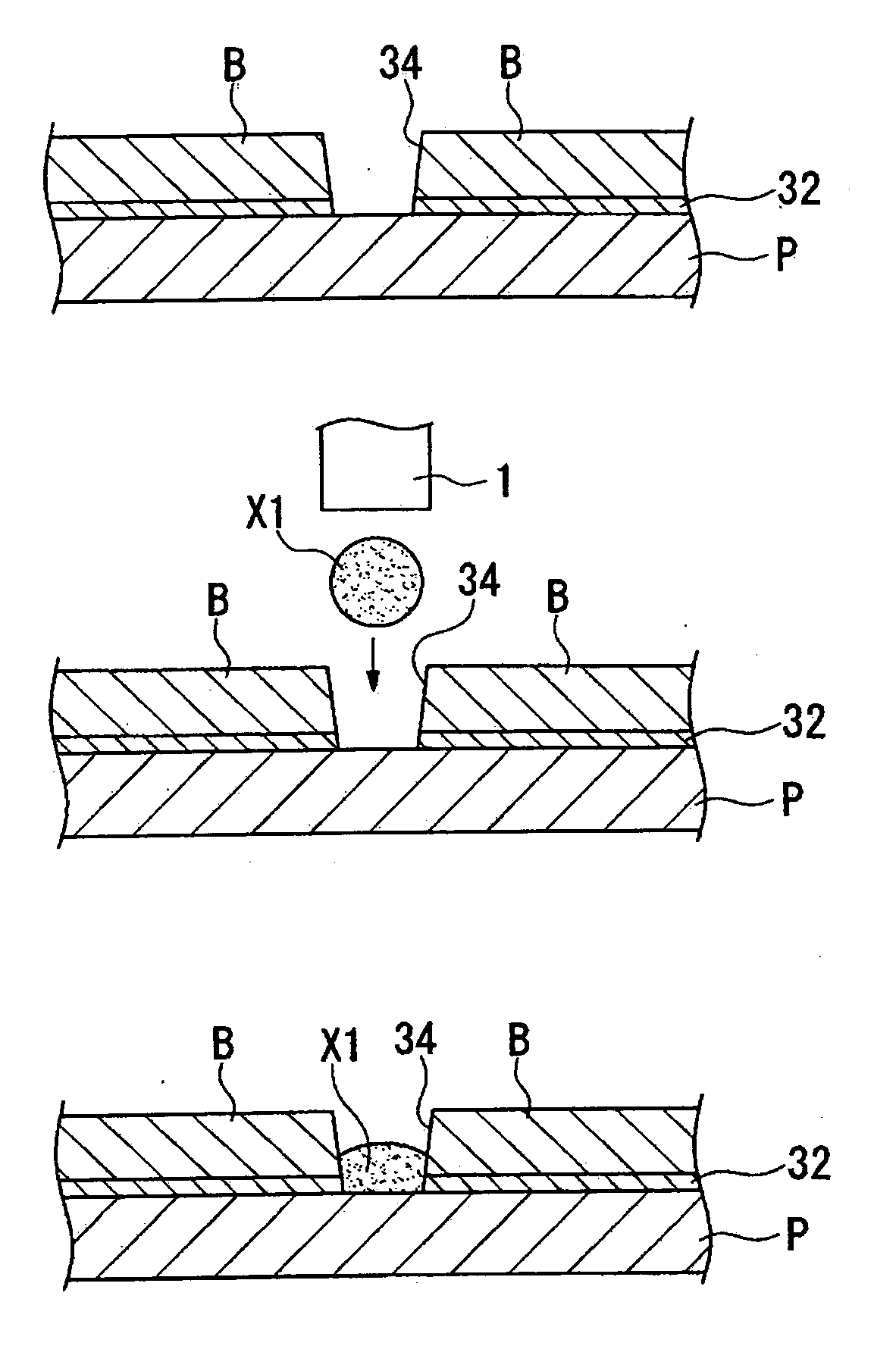
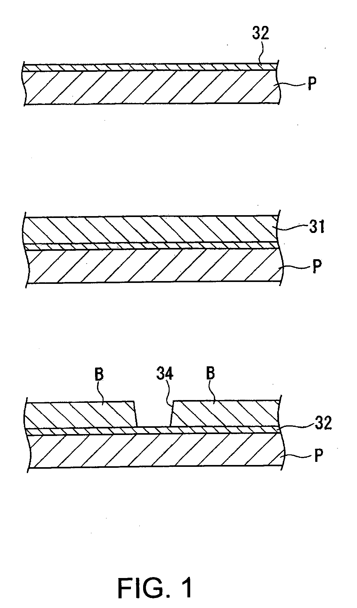
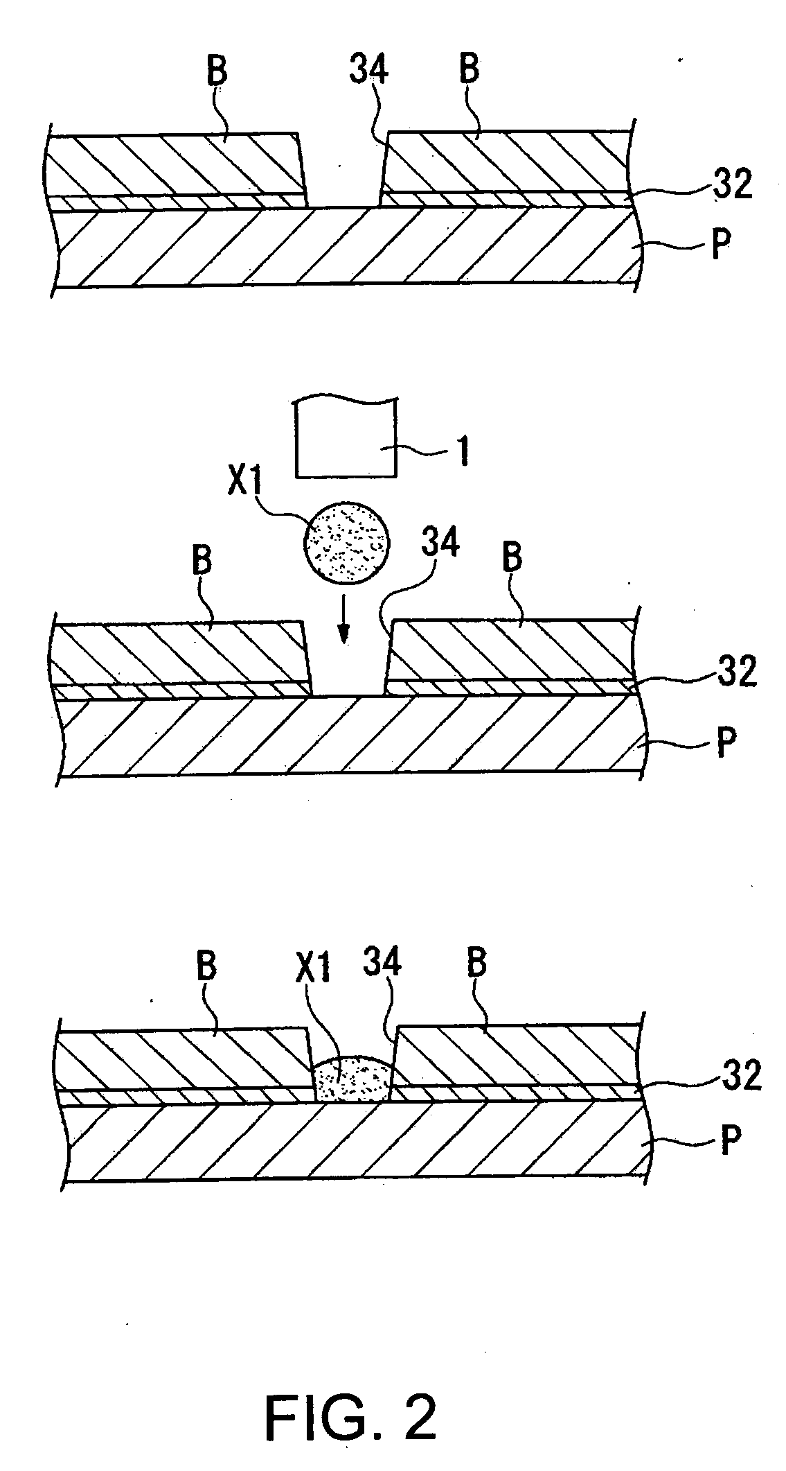
[0024] Embodiments of the invention will be described below with reference to the drawings. It should be noted that in each drawing, a different scale is used for each layer and each part to present each layer and each part in recognizable size on the drawings.

[0025] First, an embodiment of a method for manufacturing a functional film of the invention will be described. In the following manufacturing method, a bank is formed so that a wiring pattern (functional film) is formed in a region surrounded by the bank by using a droplet discharge method with a droplet discharge device. Hereinafter, each of these processes is described in detail.

[0026] In the method for forming the wiring pattern (functional film) according to the embodiment, after disposing a first ink for wiring pattern on a substrate, a second ink for wiring pattern is disposed. The method is roughly composed of a HMDS film forming process, a bank forming process, a residue treatment process (lyophilic process), a lyop...


PUM

PropertyMeasurementUnit
melting pointaaaaaaaaaa
diameteraaaaaaaaaa
melting pointaaaaaaaaaa

Abstract

A method for manufacturing a functional film, including disposing a first ink on a substrate and disposing a second ink on the first ink that has been disposed, the first ink containing at least one of a metal and a metal oxide as a solute, the metal and the metal oxide having a melting point of 900 degrees and above in bulk, upon making the metal and the metal oxide to a particle of having a diameter of from 30 to 150 nm, the particle having a melting point of 255 degrees centigrade and above, and the second ink containing an organic metal salt as a solute.

Description

BACKGROUND OF THE INVENTION [0001] 1. Technical Field [0002] The present invention relates to a method for manufacturing a functional film and a method for manufacturing a thin film transistor. [0003] 2. Related Art [0004] A photolithographic method is used in the process for forming electrodes or wirings, etc., when thin film transistors (TFTs) are manufactured that serve as switching elements used in electro-optical devices such as liquid crystal devices, etc. Circuit patterns of a functional film are formed by the photolithographic method as following: the functional film is formed existing film forming methods such as spattering or CVD in advance; a photosensitive material called a resist is coated on a substrate; the circuit patterns are exposed and developed; and the functional film is etched corresponding to resist patterns. The forming and patterning of the functional thin film using the series of photolithography methods, however, have the following disadvantages: large-sca...

Claims


Application Information

Patent Timeline
Patent Type & Authority Applications(United States)
IPC IPC(8): B05D3/02
CPCH01L29/458H01L27/1292H01L51/0022H10K71/611H01L21/288
Inventor DENDA, ATSUSHI
Owner SEIKO EPSON CORP
Why Eureka
Try Eureka