Antistatic layer for electrically modulated display

a charge control and antistatic layer technology, applied in the direction of photosensitive materials, discharge tubes, luminescent screens, etc., can solve the problems of affecting the display quality, so as to prevent uncontrolled localized static buildup, friction control, and sufficient conductivity

Inactive Publication Date: 2006-03-30
EASTMAN KODAK CO
View PDF18 Cites 27 Cited by
  • Summary
  • Abstract
  • Description
  • Claims
  • Application Information

AI Technical Summary

Benefits of technology

[0010] The present invention includes several advantages, not all of which are incorporated in a single embodiment. The inclusion of an antistatic layer with sufficient conductivity and in an electrically modulated imaging element is essential to prevent uncontrolled localized static buildup that can cause electrically modulated imaging layers to switch states. The present invention may also provide additional benefits in friction control, scratch resistances, light stability of liquid crystals, less unwanted dirt and improved transport through finishing and cutting equipment.

Problems solved by technology

The problem of controlling static charge during plastic web manufacturing and transport is well known.
Generation and uncontrolled discharge of electrostatic charge can cause a number of serious problems including safety hazards.
In the field of imaging, particularly photography and displays with an electrically modulated imaging layer, the accumulation of charge on surfaces leads to the attraction of dirt, which can produce physical defects.
The resulting web has a static induced mark that is in a different state than the surrounding background, creating a defect in the web.
In many cases the switched portion of liquid crystal cannot be switched back easily.
However, many of the inorganic salts, polymeric electrolytes, and low molecular weight surfactants used are water-soluble and are leached out of the antistatic layers during processing, resulting in a loss of antistatic function.
However, these antistatic layers typically contain a high volume percentage of electronically conducting materials, which are often expensive and impart unfavorable physical characteristics, such as color, increased brittleness, and poor adhesion to the antistatic layer.
Under fast drying conditions, as dictated by efficiency, formation of such layers may pose some problems.
An improper drying will invariably cause coating defects and inadequate adhesion and / or cohesion of the antistatic layer, generating waste or inferior performance.
Poor adhesion or cohesion of the antistatic layer can lead to unacceptable dusting and track-off.
A discontinuous antistatic layer, resulting from dusting, flaking, or other causes, may exhibit poor conductivity, and may not provide necessary static protection.
Improper drying can also allow leaching of calcium stearate from the paper support into the processing tanks, causing build-up of stearate sludge.
Flakes of the antistatic backing in the processing solution can form soft tar-like species, which, even in extremely small amounts, can re-deposit as smudges on drier rollers, eventually transferring to image areas of the photographic paper, creating unacceptable defects.
Moreover, the majority of conductive materials used as antistats on current photographic paper products lose their electrical conductivity after photographic processing due to their ionic nature.
This can cause print sticking after drying in the photo processor, and / or in a stack.
These materials are also very expensive when compared to more conventional conductive compounds.

Method used


Image

  • Antistatic layer for electrically modulated display

Examples


example 1 (

CONTROL)

[0109] A liquid crystal display was prepared as follows: A 125 micron polyethylene terephthalate substrate was coated with a layer of ITO (300 ohm per square resistivity) forming the first electrode (conductive layer) on one side of the substrate. The ITO was laser etched with thin lines to electrically separate rows in the first electrode with each row corresponding to an individual character in the display. An imageable layer containing gelatin and droplets of cholesteric liquid crystal was coated on the ITO layer. A color contrasting black layer containing gelatin and cyan, magenta, yellow, and black pigments was coated on the imageable layer. Thin bands of the two coated layers were removed along an edge of the display perpendicular to the laser etch lines. This exposed the ITO along the edge of the display to allow electrical contact to the first electrode.

example 2 (

INVENTION)

[0110] A liquid crystal display was prepared as follows: A 125 micron polyethylene terephthalate substrate was coated with a layer of ITO (300 ohm per square resistively) forming the first electrode on one side of the substrate and a transparent antistatic layer was coated on the side opposite the ITO layer. The ITO was laser etched with thin lines to electrically separate rows in the first electrode. Each row corresponds to an individual character in the display. The transparent antistatic layer was formed by coating an aqueous composition comprising a binder and a conductive antistatic agent with a weight ratio of 40:60, resulting in a layer with resistivity of 1.6×10¹⁰ log ohms per square. Polyethyleneimine (such as Mica A-131-X, supplied by the Mica Corporation) was used as the polymeric binder, and a cross-linked vinylbenzyl quaternary ammonium polymer is used as the conductive antistatic agent. An imageable layer containing gelatin and droplets of cholesteric liquid ...

example 3 (

INVENTIVE) (SINGLE LAYER COATING OF UV ABSORBER AND ANTISTATS)

[0111] Coating solution A (preparation described below) was coated on bare 4 mil poly(ethylene terephthalate (PET) film substrate at 2.0 cc / ft2 wet coverage to obtain a layer of approximately 2.4 μm thick. Corona discharge treatment at 100 jouls / ft2 was applied to the coating surface of PET film prior to coating to improve adhesion. The ITO side of the substrate was laser etched with a series parallel line with the laser etching the ITO in a continuous connected line.

Coating solution A (all refers to weight percentage of active ingredient in final solution)

[0112] 0.3125% polythiophene (active ingredient of Baytron P, available from Bayer)

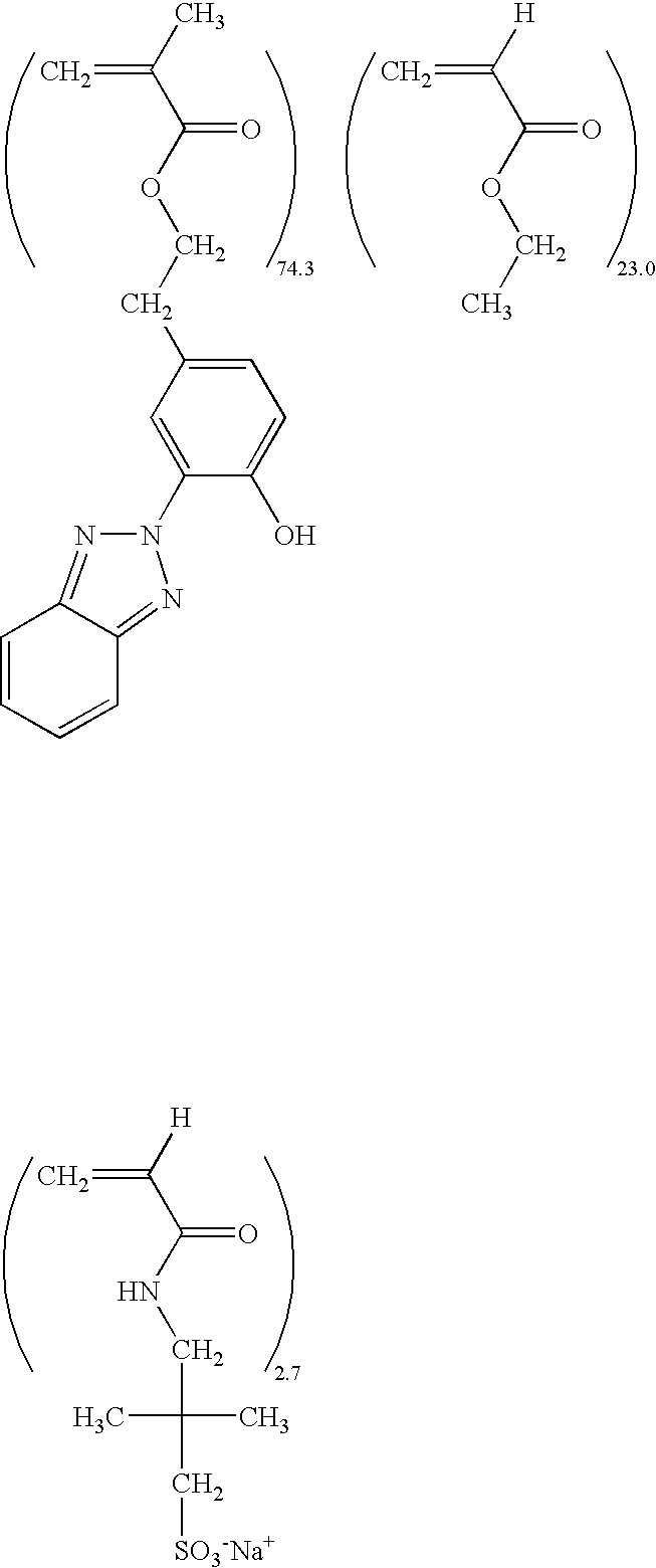
[0113] 5.9375% polyurethane (Sancure 898, available from Noveon) 5.00% UV latex

[0114] 0.5% CX-100 (polyurethane crosslinking agent, which is a polyfunctional aziridine crosslinker for the polyurethane-acrylic copolymer dispersion, obtained from Neo Resins (a division of Avecia)

[0115...


PUM

PropertyMeasurementUnit
wavelengthsaaaaaaaaaa
surface roughnessaaaaaaaaaa
thicknessaaaaaaaaaa

Abstract

The present invention relates to a display comprising at least one substrate having at least one electrically modulated imaging layer thereon, at least one patterned electrically conductive layer, and at least one antistatic layer.

Description

FIELD OF THE INVENTION [0001] The present invention relates to antistatic and charge control layers on displays with an electrically modulated imaging layer to prevent static induced switching. BACKGROUND OF THE INVENTION [0002] The problem of controlling static charge during plastic web manufacturing and transport is well known. Generation and uncontrolled discharge of electrostatic charge can cause a number of serious problems including safety hazards. In the field of imaging, particularly photography and displays with an electrically modulated imaging layer, the accumulation of charge on surfaces leads to the attraction of dirt, which can produce physical defects. The discharge of accumulated charge during or after the application of the electrically modulated imaging layer or layer(s) can produce irregular switch patterns or “static marks” in the electrically modulated imaging layer. The static problems have been aggravated by increased sensitivity of new liquid crystals, increa...

Claims


Application Information

Patent Timeline
Patent Type & Authority Applications(United States)
IPC IPC(8): C09K19/00G03C5/00
CPCG02F1/1333G02F1/133305G02F2001/133334Y10T428/1082Y10T428/10Y10T428/1059Y10T428/1086G02F2202/22C09K2323/059C09K2323/05C09K2323/06C09K2323/00G02F1/133334
Inventor AYLWARD, PETER T.MAJUMDAR, DEBASISYAU, HWEI-LINGDURKIN, WILLIAM J.BIGELOW, DONALD O.SLATER, DANIEL A.ROBINSON, KELLY S.
Owner EASTMAN KODAK CO
Why Eureka
Try Eureka