Plating substrate, electroless plating method, and circuit forming method using the same

a technology of electroless plating and substrate, applied in the direction of transportation and packaging, chemical coating, liquid/solution decomposition, etc., can solve the problems of limiting the formation of fine pitch wiring patterns, affecting so as to improve the high frequency properties of the circuit and improve the gold plating film

Inactive Publication Date: 2006-04-27
ALPS ALPINE CO LTD
View PDF6 Cites 22 Cited by
  • Summary
  • Abstract
  • Description
  • Claims
  • Application Information

AI Technical Summary

Benefits of technology

[0014] Accordingly, the present invention was made in consideration of the problems described above, and it is an object of the present invention to provide a plating substrate, an electroless plating method, and a circuit forming method using the aforementioned method. In the plating substrate described above, a copper plating film can be favorably adhered to a mirror-finished surface of a base material so as to form a fine pitch wiring pattern, and hence a circuit having superior high frequency properties can be formed.

Problems solved by technology

However, when the copper plating film, which is provided on the surface of the ceramic base material processed by the roughening treatment, is used as an electrode of a dielectric resonator or the like, an electrode having a wiring pattern with a pitch of approximately 100 μm may be formed; however, it becomes difficult to form an electrode having a wiring patter with a pitch of approximately 20 μm, and as a result, there has been a limit to form an electrode having a fine pitch wiring pattern.
In addition, in the dielectric resonator as described above, the Q is decreased in a non-load state, and as a result, high frequency properties are disadvantageously degraded.
Furthermore, the problem described above becomes more serious when coarser irregularities are formed on the surface by surface roughening treatment.
In addition, since hydrogen fluoride is used in one step of the roughening treatment, waste disposal treatment is also required, the number of production steps is increased, and as a result, the production cost is disadvantageously increased.
However, when a copper plating film is formed on a mirror-finished surface of the ceramic base material, a problem may arise in that the adhesion of the copper plating film to the surface is considerably decreased.

Method used


Image

  • Plating substrate, electroless plating method, and circuit forming method using the same
  • Plating substrate, electroless plating method, and circuit forming method using the same
  • Plating substrate, electroless plating method, and circuit forming method using the same

Examples


example 1

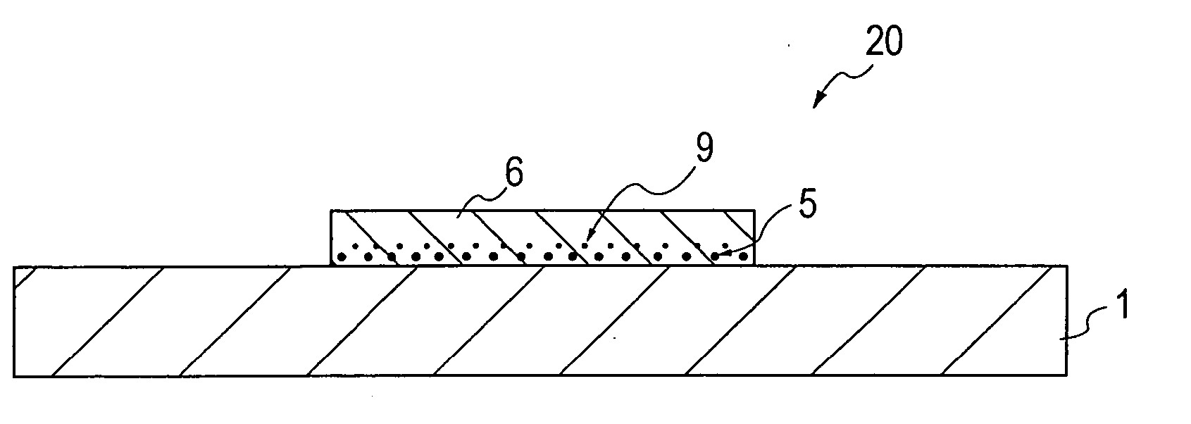
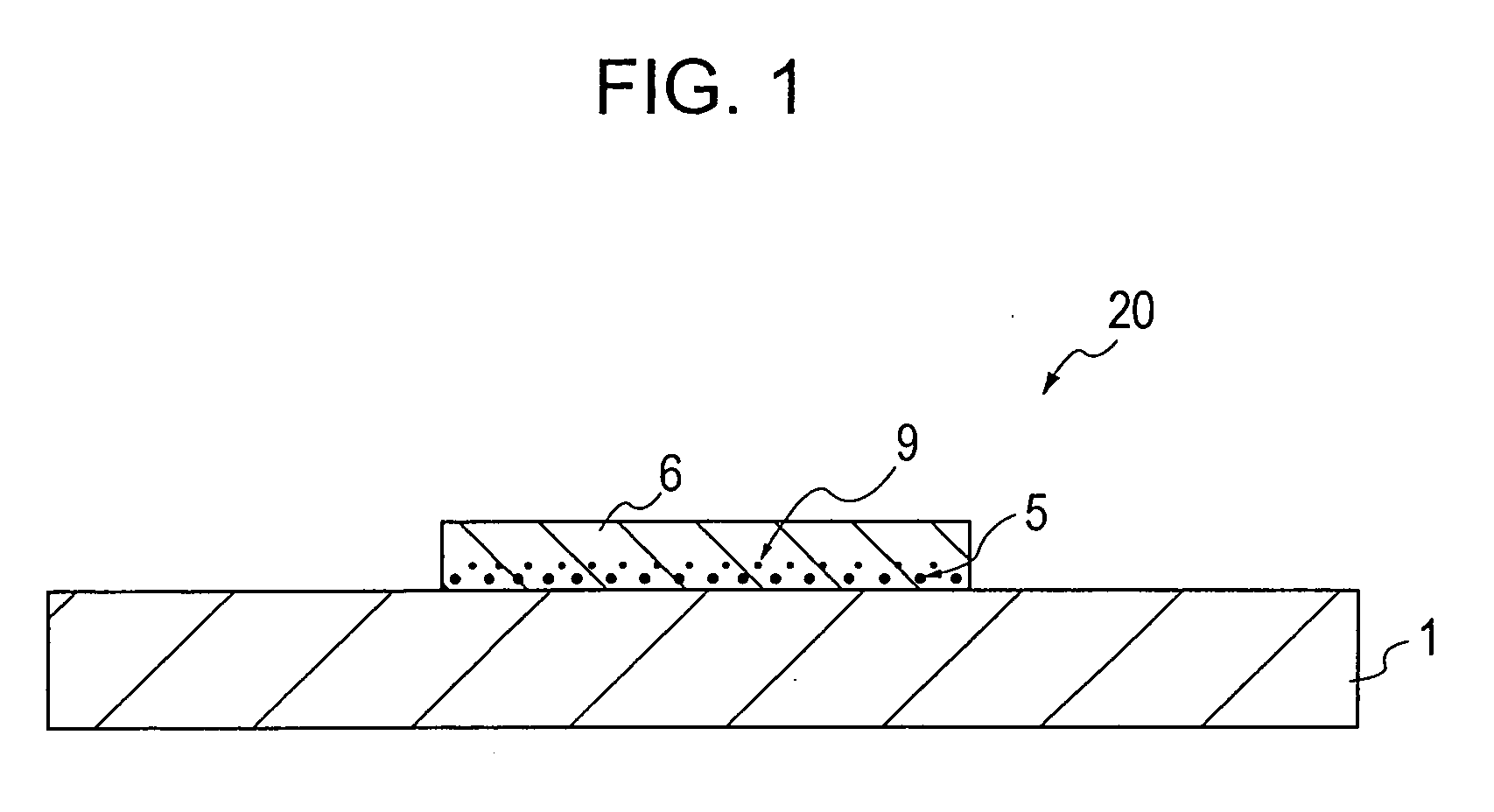
[0222] Approximately 50% of a borosilicate glass and approximately 50% of a fine alumina powder were mixed to form ceramic base materials each containing a glass component, and the ceramic base materials thus formed were degreased and washed.

[0223] Next, the ceramic base materials thus degreased and washed were immersed in the aqueous tin chloride solution of the first embodiment at 23° C. for 3 minutes, followed by sufficient washing with water. In addition, the ceramic base materials thus washed were then immersed in the aqueous palladium chloride solution described in the first embodiment at 30° C. for 2 minutes.

[0224] Furthermore, the ceramic base materials were again immersed in the above aqueous tin chloride solution for 2 minutes and then immersed in the above aqueous palladium chloride solution for 1 minute to form catalyst layers and were sufficiently washed with water, followed by drying.

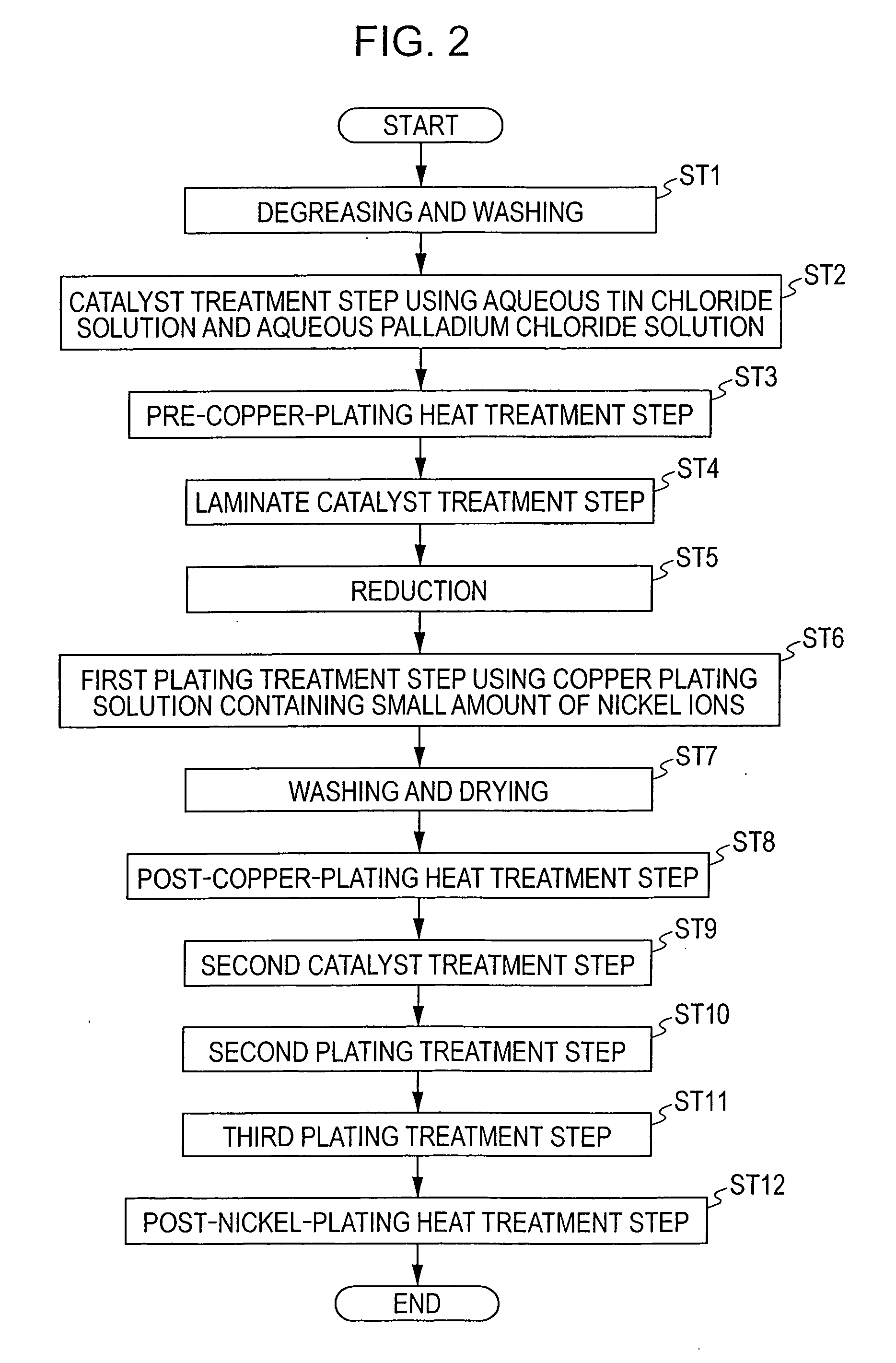
[0225] Subsequently, as shown in Table 1, pre-copper-plating heat treatment was per...

example 2

[0236] Approximately 50% of a borosilicate glass and approximately 50% of a fine alumina powder were mixed to form a ceramic base material containing a glass component, and the ceramic base material thus formed was degreased and washed.

[0237] Next, after being applied onto a first and a second surface of the ceramic base material, a resist solution was processed by exposure and development using a predetermined mask so as to form resists having a predetermined pattern, followed by sufficient washing with water.

[0238] Subsequently, the ceramic base material was immersed in the aqueous tin chloride solution described in the circuit forming method using the electroless plating method of the first embodiment for 3 minutes, followed by sufficient washing with water. In addition, the ceramic base material thus washed was then immersed in the aqueous palladium chloride solution described in the first embodiment for 2 minutes.

[0239] Furthermore, the ceramic base material was again immers...

example 3

[0249] Ceramic base materials containing a glass component, which were each formed of approximately 50% of a borosilicate glass and approximately 50% of a fine alumina powder and which were each provided with Ag-based vias therein, were degreased and washed using a degreasing agent containing sodium hydroxide, a carbonate, a phosphate, and the like.

[0250] Subsequently, ceramic base materials were immersed in the aqueous tin chloride solution described in the second embodiment at 23° C. for 3 minutes, followed by sufficient washing with water. In addition, the ceramic base materials thus washed were then immersed in the aqueous palladium chloride solution described in the second embodiment at 30° C. for 2 minutes. Furthermore, the ceramic base materials were again immersed in the above aqueous tin chloride solution for 2 minutes and were then immersed in the above aqueous palladium chloride solution for 1 minute to form catalyst layers, followed by sufficient washing with water and ...


PUM

PropertyMeasurementUnit
temperatureaaaaaaaaaa

Abstract

An electroless copper plating method is provided having a first catalyst step of forming a first catalyst layer on a ceramic base material containing a glass component using a tin chloride solution and a palladium chloride solution; a pre-copper-plating heat treatment step of heating the ceramic base material in an atmosphere containing oxygen; a laminate catalyst treatment step of forming a laminate catalyst layer on the ceramic base material using a tin chloride solution and a palladium chloride solution; a plating treatment step of forming a copper plating film on the ceramic base material using a copper plating solution containing a small amount of nickel ions; and a post-copper-plating heat treatment step of heating the ceramic base material at a heat treatment temperature not more than the glass transition temperature thereof.

Description

BACKGROUND OF THE INVENTION [0001] 1. Field of the Invention [0002] The present invention relates to a plating substrate composed of a copper plating film provided on a glass base material or a ceramic base material, having at least an oxide on a surface thereof, an electroless plating method forming a copper plating film, and a circuit forming method using the aforementioned method. [0003] 2. Description of the Related Art [0004] Heretofore, for example, as a method for forming a plating film on a glass base material or a ceramic base material, an electroless copper plating method has been known (for example, see Japanese Unexamined Patent Application Publication Nos. 2000-54153, 2003-13247, and 2004-332023). [0005] In a related electroless copper plating method, in order to ensure high adhesion between a surface of a base material and a copper plating film formed thereon by an anchor effect, first, the surface is intensively processed by surface roughening treatment, so that coars...

Claims


Application Information

Patent Timeline
Patent Type & Authority Applications(United States)
IPC IPC(8): B32B3/00B32B18/00B32B17/06B32B15/04B32B9/00B32B19/00
CPCC03C17/40Y10T428/12611C23C18/1651C23C18/1692C23C18/1879C23C18/1889C23C18/32C23C18/405C23C18/42C23C18/48H05K1/0306H05K3/181H05K2203/1105Y10T428/24917Y10T428/24926Y10T428/12597Y10T428/12903C03C2218/115
Inventor MITSUMORI, KENICHI
Owner ALPS ALPINE CO LTD
Why Eureka
Try Eureka