Method for fabricating polymer optical waveguide device

a technology of optical waveguides and polymers, applied in the direction of optical waveguide light guides, instruments, domestic applications, etc., can solve the problems of increasing production costs, affecting the accuracy of the resultant core diameter, and bonding films together, and achieves low light loss, high functional optical circuit base materials, and simple fabrication.

Inactive Publication Date: 2006-05-04
FUJIFILM BUSINESS INNOVATION CORP
View PDF4 Cites 41 Cited by
  • Summary
  • Abstract
  • Description
  • Claims
  • Application Information

AI Technical Summary

Benefits of technology

[0021] In a polymer optical waveguide device fabricated according to the invention, the polymer optical waveguide may be formed on the cladding base material in advance, and an optical device is inserted into an optical device inserting portion (space, groove) that is formed in the highly precise optical waveguide in advance, a predetermined optical adhesive is incorporated into the optical pathway between the waveguide (core portion) on the waveguide base material and the optical device, and the adhesive is optically hardened, thereby enabling simple fabrication of a highly functional optical circuit base material. In addition, each electronic device can also be placed on the surface of the optical circuit base material in close proximity, whereby a photoelectric consolidation type circuit base material, in which optical and electronic devices are consolidated with a low loss of light and highly densely, can readily be fabricated.
[0022] In particular, causing the properties (hardness, material, thickness, surface energy, surface smoothness) of a hardened resin layer, which is a mold, to be in a constant range enables easy attainment of a high quality waveguide at a low cost. Additionally, the shape of an optical waveguide to be formed can be freely designed, thereby achieving optical properties of extremely precise shape reproduction and low loss wave guiding, despite the manufacturing process being easy and simple. Moreover, a variety of optical devices can freely and easily be attached, providing with great precision a fundamental form of a highly functional optical circuit base material.

Problems solved by technology

However, selective polymerization as in (1) above poses a problem in bonding films together.
The methods of (2) and (3) increase production costs due to the use of photolithography.
The method of (4) causes a problem in precision of a resultant core diameter.
The method of (5) presents a problem in that the method cannot produce a sufficient refractive index difference between the core portion and the cladding layer.
At present, examples of practical methods that are excellent in performance of the waveguide include only the methods of (2) and (3); however, they pose problems in production costs as noted supra.
Further, all methods (1) to (5) are difficult to apply to the formation of polymer waveguides in a plastic base material that has a large area and is flexible.
This presents a problem in that light leaks through this thin layer.
The light wiring devices described in JP-A Nos. 2000-39530 and 2000-39531 have complex constructions, and thus their fabrication requires very complicated processes.
JP-A No. 2000-235127 discloses an optoelectronic integrated circuit in which a polymer optical waveguide circuit is directly patterned on top of a photoelectric fusion circuit produced by integrating electronic devices and optical devices; however, photolithography, which is costly, is used for the fabrication of the polymer optical waveguide.
Hence, the optoelectronic integrated circuit is inevitably high-priced.
In this respect, conventional inorganic type optical waveguides pose many problems in that the loss of light is large due to the insertion of an optical device.

Method used


Image

  • Method for fabricating polymer optical waveguide device
  • Method for fabricating polymer optical waveguide device
  • Method for fabricating polymer optical waveguide device

Examples


example 1

Production of a Mold

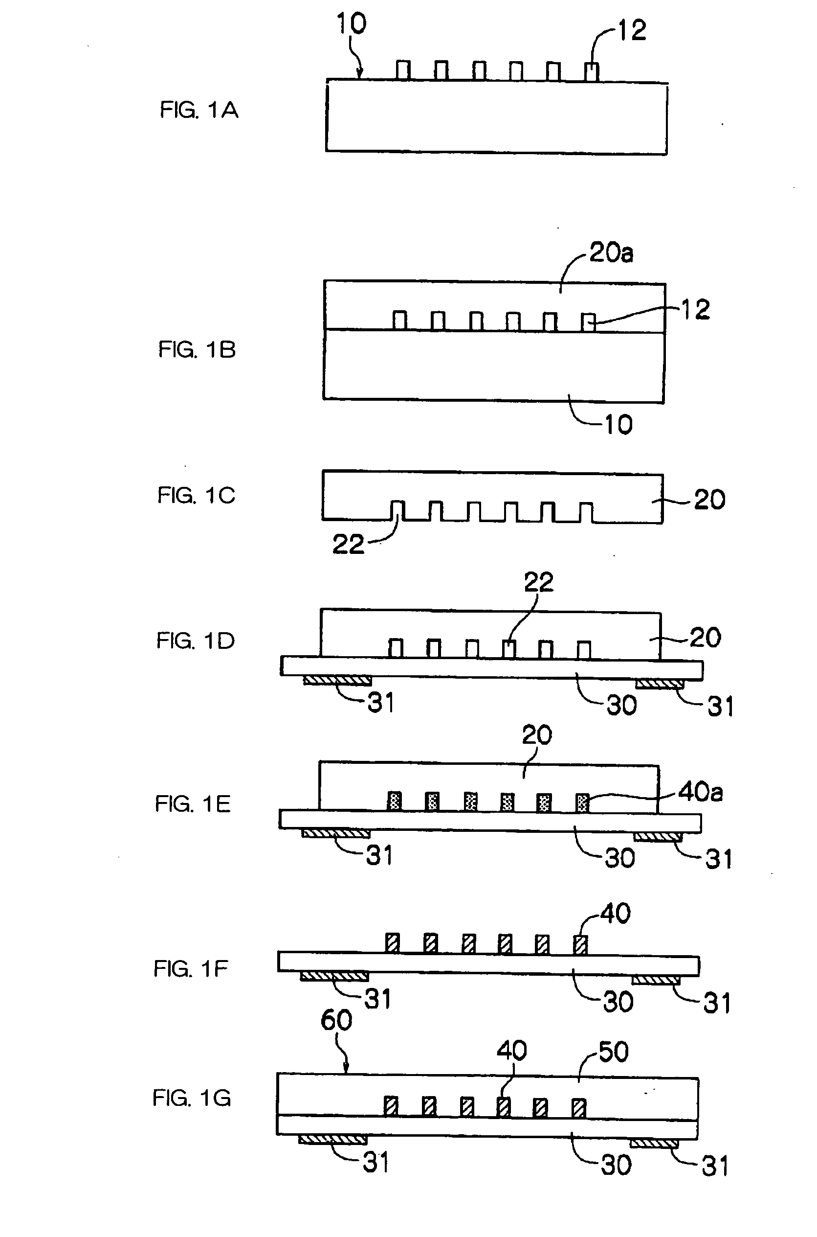
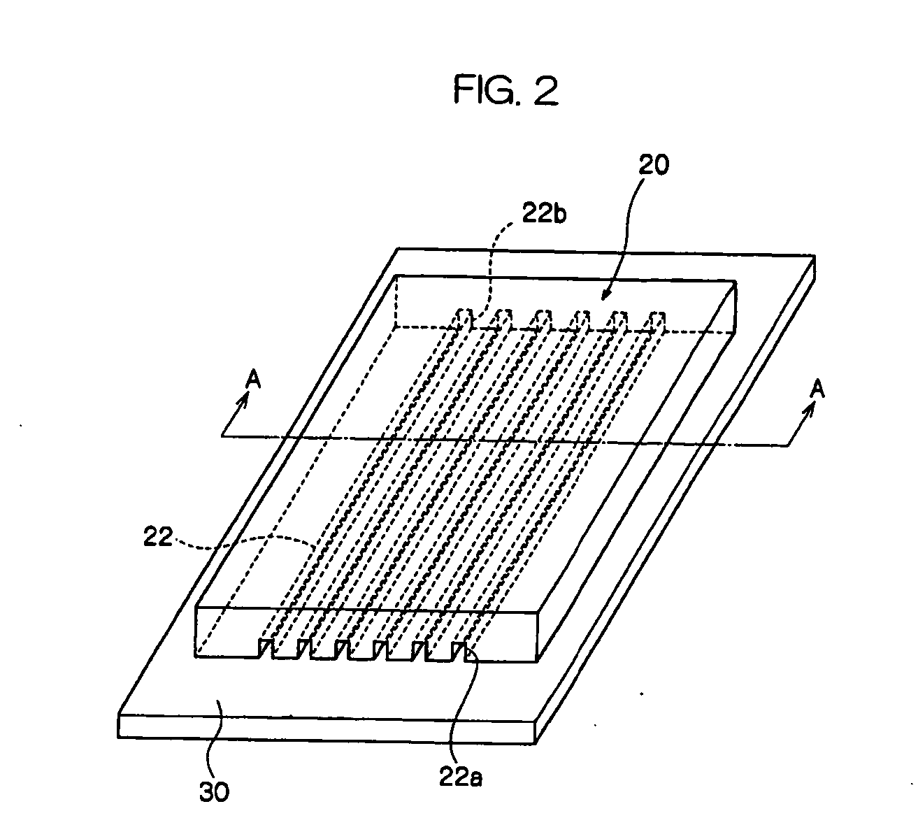
[0152] An ultraviolet ray curing thick film resist (trade name: SU-8, manufactured by Micro Chemical Inc.) is applied to the surface of a quartz base material by spin coating and the resulting material is pre-baked in a heating oven. Five convex portions (width: 50 μm, height: 50 μm, pitch: 250 μm, length: 50 mm) made of an ultraviolet ray cured polymer material having the cross-section of a square are patterned on the material by a photolithographic process to fabricate a matrix for the production of a mold.

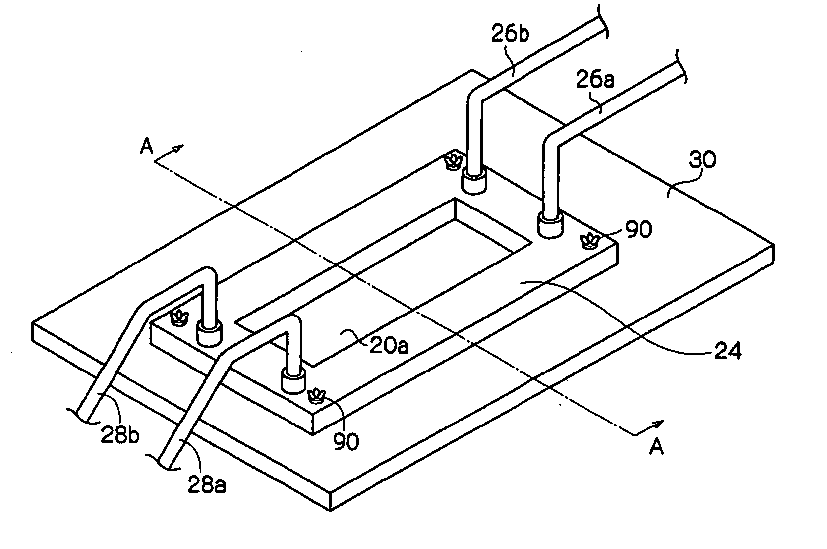
[0153] Next, an opening portion through which ultraviolet rays are transmitted is provided as shown in FIG. 4A, and a reinforcing member (made of aluminum strip having a thickness of 1.5 mm) having three injection ports and three discharge ports is prepared, and then five concave portions (width: 100 μm, height: 100 μm, pitch: 500 μm, length: 50 mm) having a shape similar to the concave portions correspondent to the above-described convex portions are prod...

example 2

[0161] A polymer optical waveguide is fabricated as in Example 1 with the exception that the hardness of the cured resin layer as the mold is 80 in terms of shore A hardness. In addition, the hardness of the silicone rubber material, the cured resin layer, is adjusted by the amount of a ceramic ultra fine powder that is added to the aforementioned liquid dimethylsiloxane rubber.

[0162] Of the five resulting core portions, the mean wave guide loss of three optical waveguide core portions is 1.8 dB / cm; no optical guide waves can be confirmed for the other two.

[0163] Next, a groove is produced in the waveguide base material as in Example 1 and a wavelength selecting optical filter is bonded thereto. The result is that the loss of light after wavelength selection in the three core portions that have confirmed the aforementioned optical guide waves is 5.9 dB.

example 3

[0164] A polymer optical waveguide is fabricated as in Example 1 with the exception that the hardness of the cured resin layer as the mold is 30 in terms of shore A hardness. The mean guide wave loss of the polymer optical waveguide is 0.15 dB / cm.

[0165] Next, a groove having a mean width of 1.15 mm is formed to a length of 20 mm on the waveguide base material so as to cut the core portions, at an angle of 45 degrees relative to the waveguide base material surface, as shown in FIGS. 7B and 7C, by dicing by means of a dicer apparatus having a dicer blade of a thickness of 1.0 mm. Then, into this groove a wavelength selecting optical filter with a thickness of 0.5 mm that reflects light having a wavelength of 1.3 μm and transmits light having a wavelength of 0.85 μm is inserted, and the optical filter is positioned in such a way that the maximum void width between the cut core portion ends and the optical pathway portions of the wavelength selecting optical filter is 0.90 mm (mean voi...


PUM

PropertyMeasurementUnit
lengthaaaaaaaaaa
mean roughnessaaaaaaaaaa
void widthaaaaaaaaaa

Abstract

The present invention provides a method for fabricating a polymer optical waveguide device, the method at least includes: preparing a mold including a cured resin layer of a mold forming curing resin and having a concave portion correspondent to a core portion of an optical waveguide formed therein; attaching the mold to a cladding base material; filling the concave portion of the mold with a core forming curing resin; hardening the core forming curing resin to form a cured core portion; forming a space or a groove for placing an optical device in a middle part in the waveguide direction of the core portion such that the optical device cuts across the core portion; inserting and positioning the optical device in a predetermined position of the space or groove; and conducting an optical bonding between an optical pathway portion of the optical device and the core portion.

Description

CROSS-REFERENCE TO RELATED APPLICATION [0001] This application claims priority under 35 USC 119 from Japanese Patent Application No. 2004-315758, the disclosure of which is incorporated by reference herein. BACKGROUND OF THE INVENTION [0002] 1. Field of Invention [0003] The present invention relates to a method for fabricating a polymer optical waveguide device provided with an optical device. [0004] 2. Description of the Related Art [0005] The methods for producing polymer waveguides that have been proposed include, for example, (1) a method that involves impregnating films with a monomer, selectively exposing the core portion to light to change the refractive index of the core portion, and then bonding the films together (selective polymerization); (2) a method that involves molding a core layer and a cladding layer by coating and subsequently forming a cladding portion by means of reactive ion etching (RIE method); (3) a method that involves adding a photosensitive material to a ...

Claims


Application Information

Patent Timeline
Patent Type & Authority Applications(United States)
IPC IPC(8): B29D11/00
CPCB29D11/00663
Inventor AKUTSU, EIICHIOHTSU, SHIGEMISHIMIZU, KEISHIYATSUDA, KAZUTOSHI
Owner FUJIFILM BUSINESS INNOVATION CORP
Why Eureka
Try Eureka