Near single-crystalline, high-carrier-mobility silicon thin film on a polycrystalline/amorphous substrate

a polycrystalline/amorphous substrate, high carrier mobility technology, applied in the field of materials, can solve the problems inability to find suitable epitaxial template for well-oriented film growth, and inability to meet the requirements of a single crystal template, etc., to achieve the effect of low chemical reactivity

Inactive Publication Date: 2006-06-01
LOS ALAMOS NATIONAL SECURITY
View PDF3 Cites 68 Cited by
  • Summary
  • Abstract
  • Description
  • Claims
  • Application Information

AI Technical Summary

Benefits of technology

[0010] The present invention further provides a process of preparing a semiconductor article including depositing a buffer material layer onto a base substrate including: (i) a base material selected from the group consisting of polycrystalline substrates and amorphous substrates, and (ii) at least one layer of a differing material upon the surface of the base material, the buffer material layer characterized by: (a) low chemical reactivity with the base substrate, (b) stability at temperatures up to at least about 800° C. under low vacuum conditions, and (c) a lattice crystal structure adapted for subsequent deposition of a semiconductor material; and, depositing a layer of a biaxially oriented semiconductor material onto the buffer material layer

Problems solved by technology

In many thin film semiconductor applications, including sensor and other devices, a major technical difficulty is the lack of a suitable epitaxial template for the growth of well-oriented films.
Favorable device characteristics are generally better defined and more pronounced in well-oriented (i.e., nearly single-crystalline) thin films, but conventional epitaxial film-growth techniques require single crystal templates that are either expensive or of limited availability or both.
Grain boundaries in polycrystalline semiconductor films can result in local lattice distortions and dangling bonds.

Method used


Image

  • Near single-crystalline, high-carrier-mobility silicon thin film on a polycrystalline/amorphous substrate
  • Near single-crystalline, high-carrier-mobility silicon thin film on a polycrystalline/amorphous substrate
  • Near single-crystalline, high-carrier-mobility silicon thin film on a polycrystalline/amorphous substrate

Examples


example 1

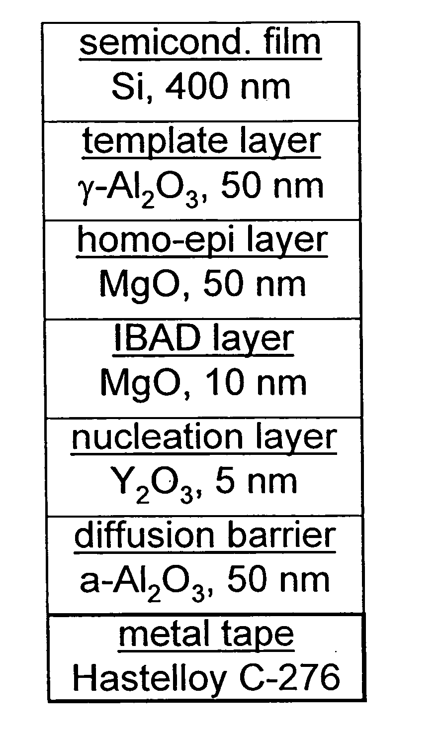
[0033] A structure in accordance with FIG. 1 was prepared as follows. A 1-cm-wide and 100-μm-thick nickel metal tape (Hastelloy C-276) was rolled and electrochemically polished to a root mean square (rms) surface roughness of about 1 nm, measured on a 5×5 μm2 scale.

[0034] This flexible polycrystalline metal substrate was then cleaned by an argon ion beam etch (90 mA, 750 V, 22×6-cm rf Kaufmann source). Next, a 50 nanometer (nm) thick amorphous layer of aluminum oxide (Al2O3) was deposited at room temperature by e-beam evaporation onto the nickel metal tape. Then, a 7 nm thick layer of yttrium oxide (Y2O3) was deposited at room temperature at a rate of about 0.15 nm per second (nm / s) by e-beam evaporation. Next, a 10 nm thick layer of magnesium oxide (MgO) was deposited using ion beam assisted deposition at room temperature (argon ion assist beam at 45° to substrate normal, 90 mA, 750 V) with a deposition rate of about 0.4 nm / s. A homo-epitaxial layer of MgO (from about 50 to 100 nm...

example 2

[0036] A biaxially-oriented silicon (Si) film was then grown on the γ-Al2O3 buffer / template layer at a temperature of about 780° C. in an ambient chamber pressure of 1×10⁻⁶ Torr. The doping concentration in the p-Si film was between 1016 and 1017 / cm3 and could be varied depending on the added amount of boron in the evaporation source of nominally pure Si. The RHEED patterns indicated that the Si grew with (001) orientation perpendicular to the substrate with in-plane lattice constant of 0.54 nm.

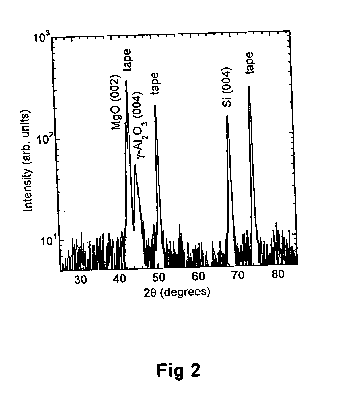
[0037] The crystallographic orientation, epitaxial relationship, and microstructure of the multilayered samples were further analyzed by x-ray diffraction (XRD) and transmission electron microscopy (TEM). An XRD θ-2θ scan (shown in FIG. 2) shows all biaxially-oriented layers (MgO, γ-Al2O3, and Si) grew with the (001) orientation perpendicular to the substrate surface. The rocking curve on the Si (004) peak yielded full width at half-maximum (FWHM) value Δω of about 0.8° (FIG. 3), whereas the...


PUM

PropertyMeasurementUnit
temperaturesaaaaaaaaaa
temperatureaaaaaaaaaa
partial pressuresaaaaaaaaaa

Abstract

A template article including a base substrate including: (i) a base material selected from the group consisting of polycrystalline substrates and amorphous substrates, and (ii) at least one layer of a differing material upon the surface of the base material; and, a buffer material layer upon the base substrate, the buffer material layer characterized by: (a) low chemical reactivity with the base substrate, (b) stability at temperatures up to at least about 800° C. under low vacuum conditions, and (c) a lattice crystal structure adapted for subsequent deposition of a semiconductor material; is provided, together with a semiconductor article including a base substrate including: (i) a base material selected from the group consisting of polycrystalline substrates and amorphous substrates, and (ii) at least one layer of a differing material upon the surface of the base material; and, a buffer material layer upon the base substrate, the buffer material layer characterized by: (a) low chemical reactivity with the base substrate, (b) stability at temperatures up to at least about 800° C. under low vacuum conditions, and (c) a lattice crystal structure adapted for subsequent deposition of a semiconductor material, and, a top-layer of semiconductor material upon the buffer material layer.

Description

[0001] This invention is the result of a contract with the United States Department of Energy (Contract No. W-7405-ENG-36). The government has certain rights to this invention.FIELD OF THE INVENTION [0002] The present invention relates to generally to the field of materials. More particularly, the invention relates to composites, articles, and / or electronic devices (such as thin film transistors and photovoltaic devices) and sensors that include nearly single-crystalline semiconductor films, e.g., silicon films or the like, on base substrates of polycrystalline or amorphous materials with suitable buffer layers thereon. BACKGROUND OF THE INVENTION [0003] High performance and low cost are the two main drivers for large scale applicability of semiconductor electronics and sensors. Thus, the challange facing the semiconductor industry is to reduce production cost while maintaining or improving device performance. In many thin film semiconductor applications, including sensor and other ...

Claims


Application Information

Patent Timeline
Patent Type & Authority Applications(United States)
IPC IPC(8): B32B13/04B32B15/04H01L21/20
CPCC30B25/18C30B29/06H01L21/0237H01L21/0242H01L21/02488H01L21/02505H01L21/02521H01L21/02532H01L21/02587H01L21/02658
Inventor FINDIKOGLU, ALP T.JIA, QUANXIARENDT, PAUL N.MATIAS, VLADIMIRCHOI, WOONG
Owner LOS ALAMOS NATIONAL SECURITY
Why Eureka
Try Eureka