Electronic device

Inactive Publication Date: 2006-08-31
HITACHI LTD
View PDF4 Cites 14 Cited by
  • Summary
  • Abstract
  • Description
  • Claims
  • Application Information

AI Technical Summary

Benefits of technology

[0027] According to the embodiment of the invention, an electronic device having suf

Problems solved by technology

If the three types of solder A to C are not used, and connection is tried to be made using the same solder at a time, various problems may occur, such as displacement of connection position due to rotation of the metal frame 21 and displacement of a connection position due to rotation of the chip 1, in addition, disconnection in the solder connecting portions (or bad conduction) and electric short circuit (short).
Moreover, if respective connecting portions are formed in the above order with the same solder, since an electronic device is subjected to heating history three times at most, growth of an intermetallic compound proceeds, the compound being derived from joints (the solder material layers) and electrodes provided on the device, causing

Method used


Image

  • Electronic device
  • Electronic device
  • Electronic device

Examples


embodiment 1

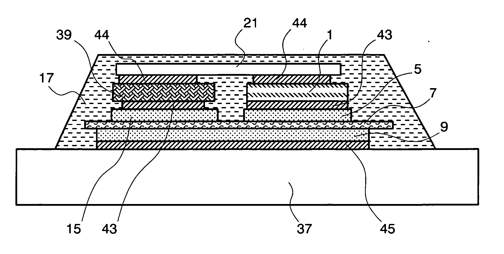
[0041] An electronic device according to the invention is described below using an embodiment suitable for realizing an electric control unit for motor control (hereinafter, abbreviated as ECU) having sufficient reliability.

[0042] First, FIG. 4 shows a schematic view of an electronic component including MOS-FET (Meal-Oxide Semiconductor Field Effect Transistor) formed on a Si base member of 5 mm on four sides and 0.3 mm in thickness (hereinafter, mentioned as MOS-FET chip or Si chip). In the MOS-FET chip, since a channel for flowing carriers (electrons and holes) in a thickness direction of a Si base member 1 is formed, two electrodes (source electrode and drain electrode) sandwiching the channel are formed on two main surfaces (top and bottom in FIG. 4) of the Si base member 1 respectively. A gate electrode for controlling flow of carriers in the channel is omitted in FIG. 4. The MOS-FET chip having such a structure is used as a power device for switching large current, for exampl...

embodiment 2

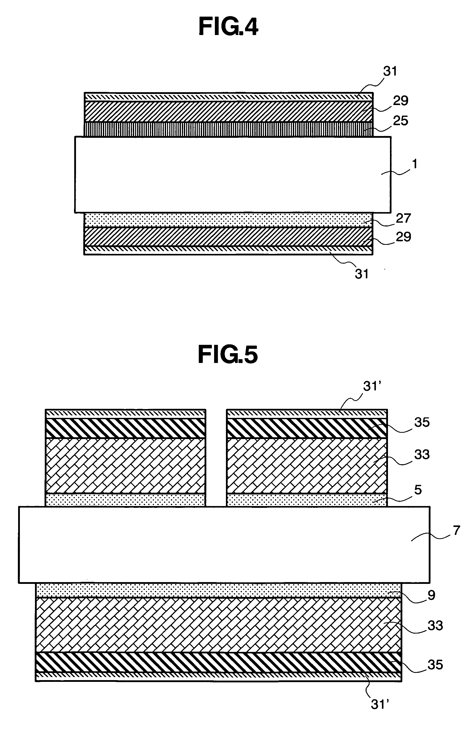
[0055] Another embodiment of an electronic device according to the invention is described below using FIG. 11. The electronic device (module) of the embodiment is different from that of the embodiment 1 in that a substrate in which one main surface of the metal base (for example, Cu base) 47 is insulated with resin 46 (called Cu base substrate for convenience) is used in place of the substrate 7 including an insulating material. In the Cu base substrate, a material having a heat conductivity of 2 W / m·K or more is used based on a demand of improving heat radiation performance in a total structure of the electronic device. Since the electronic device has the base metal 37 in the embodiment 1 within the substrate, a base substrate for heat radiation and reinforcement need not be separately provided in addition to the substrate. Therefore, the number of hierarchies of the connecting portions can be decreased one, consequently reduction in cost can be expected due to decrease in number o...

embodiment 3

[0057] Here, regarding the described embodiment 1 and embodiment 2, features of connecting portions in the electronic device according to an embodiment of the invention are considered with reference to FIG. 12(a) to FIG. 12(e).

[0058] When two members to be joined have different thermal expansion coefficients from each other, certain thickness of a connecting portion (hereinafter, described as joint layer) formed between them contributes to restrain an effect of thermal expansion (deformation) of one of the two members on the other. In the case of a Si chip and a substrate exemplified in FIG. 12(a), a thermal expansion coefficient of the former is dominated by that of silicon, and a thermal expansion coefficient of the latter is dominated by that of, for example, a ceramic material, glass epoxy material, or metal sheet as a main component of the substrate. Therefore, sometimes the joint layer is industrially requested to be formed in a thickness of at least 10 μm, and desirably 20 t...


PUM


Abstract

An electronic device according to an embodiment of the invention includes a pair of members which are connected to each other by a connecting portion layer interposed between connecting portions respectively formed thereon and have thermal expansion coefficients different from each other, wherein the connection layer is formed by diffusion reaction between the metal layers by which the metal layers are melted only in the vicinity of a contact interface between the layers, the metal layers being formed on the connecting portions with materials different from each other. At least one of the metal layers is formed by plating, thereby the connection layer is formed in a thickness sufficient to absorb difference in thermal expansion coefficient between the pair of members. Since melting temperature of the connection layer after the pair of members have been connected to each other is increased compared with melting temperature of each of the members in the diffusion reaction, the connection layer is prevented from being damaged due to heating treatment performed after the connection has been made, consequently excellent reliability of the electronic device is secured.

Description

[0001] The present application claims priority from Japanese application JP2005-052249 filed on Feb. 28, 2005, the content of which is hereby incorporated by reference into this application. BACKGROUND OF THE INVENTION [0002] 1. Field of the Invention [0003] The present invention relates to an electronic device represented by in-vehicle power module, and particularly relates to a structure of mounting an electronic component such as a semiconductor element on a substrate. [0004] 2. Description of the Related Art [0005] From consideration for environmental issues, vehicles using electric motor drive, which are represented by a hybrid electric vehicle, are expected to be increasingly widespread in future. Moreover, an electric control unit (ECU) using the electric motor tends to be used for various units that have been controlled by hydraulic pressure such as power steering or a brake system. For ECU for motor control, an IDBT (Insulated Gate Bipolar Transistor) chip or FET (Field Eff...

Claims


Application Information

Patent Timeline
IPC IPC(8): H01L23/52
CPCH01L2924/01049H01L2924/1305H01L2924/01073H01L2924/01074H01L2924/01075H01L2924/01078H01L2924/01079H01L2924/01082H01L2924/01322H01L2924/01327H01L2924/09701H01L2924/10253H01L2924/13055H01L2924/13091H01L2924/0105H01L2924/1306H01L2224/40137H01L2224/8382H01L2924/1579H01L2924/15787H01L2224/29111H01L24/29H01L24/33H01L24/40H01L24/83H01L25/072H01L2224/04026H01L2224/32225H01L2224/325H01L2224/48091H01L2224/48227H01L2224/73265H01L2224/83801H01L2924/01005H01L2924/01013H01L2924/01015H01L2924/01029H01L2924/01033H01L2924/01042H01L2924/01047H01L2924/0132H01L2924/0133H01L2224/2919H01L2924/01006H01L2924/01019H01L2924/01024H01L2924/01065H01L2924/014H01L2924/0665H01L2224/29101H01L2224/29109H01L2924/00014H01L2924/00H01L2924/01028H01L2924/00012H01L2924/3512H01L2224/40095H01L2924/181H01L2224/40225H01L24/73H01L2224/8381H01L2224/83825H01L2224/371H01L2224/84801H01L24/37H01L24/84H01L2224/2612H01L2224/73221B65G1/02
Inventor YOKOZUKA, TAKEHIDE
Owner HITACHI LTD
Why Eureka
Try Eureka