Semiconductor device and manufacturing method thereof

Inactive Publication Date: 2006-09-07
FUJITSU SEMICON LTD
View PDF25 Cites 18 Cited by
  • Summary
  • Abstract
  • Description
  • Claims
  • Application Information

AI Technical Summary

Benefits of technology

[0080] It is an object of the present invention to provide a semiconductor device and a manufacturing method thereof, wherein minute via-holes can be formed in a mass-production line without increasing parasitic capacity, increasing manufacturing steps, and causing defects.
[0082] According to another aspect of the present invention, there is provided a method of manufacturing a semiconductor device, comprising the steps of: forming a first insulating film over a semiconductor substrate; forming a second insulating film on said first insulating film; forming a third insulating film on said second insulating film, said third insulating film having a low etching rate in relation to a first etchant for said first insulating film; forming an opening portion so as to extend through said third and second insulating films up to said first insulating film; forming a spacer on the side wall of said opening portion, said spacer having a low etching rate in relation to said first etchant for said first insulating film; forming a contact hole so as to extend through said first insulating film, using said third insulating film and said spacer as masks; filling said opening portion and said contact hole with a first conductive material to form a contact plug; and selectively removing said third insulating film using a second etchant whose etching rate to said second insulating film is low.
[0084] According to the present invention, upon formation of a minute via-hole, a film transparent in relation to visible light is employed as the major part of a hard mask. Therefore, additional manufacturing steps for making it possible to detect alignment marks, can be eliminated, and thereby the throughput can be improved. This greatly contributes an improvement of reliability of highly-integrated semiconductor devices such as hybrid system LSIs with DRAMs, and an improvement of yield in manufacture.

Problems solved by technology

The above-described conventional formation methods of via-holes, however, include various problems.
This causes the problem that the capacitance between each bit line and the storage node increases.
Such an increase in capacity makes it hard to reduce the number of sense amplifier divisions.
This causes an increase in chip area.
In this case, however, the following problems arise.
As a method for forming a SiO2 film with good step coverage ability through such a low-temperature process, known is LP-TEOS method capable of forming a film at 650° C. However, the LP-TEOS film formed by this method can not be densified and reduces in its anti-breakdown property unless it is subjected to a heat treatment at about 800° C. in the atmosphere of N2.
Therefore, this method can not be used for such a hybrid system LSI including a DRAM.
No other formation method of a SiO2 film with good step coverage ability through a low-temperature process is present if mass-productivity in a factory is taken into consideration.
If the surface has been flattened, however, unevenness in height caused by the alignment marks for photolithography may disappear, and detection of the alignment marks may become impossible through the opaque film.
This may cause a metallic contamination of the depositing device for the doped amorphous Si layer for forming the Si plug in the subsequent stage.
In a usual factory, however, such a limited use of the device is hard.
This may result in generation of abnormal etching portions 70.
This causes a problem on throughput.
Besides, when a plasma CVD process is used for the hard mask and a BPSG film exists in the lower layer, the P—SiN film formed through the process may crack if its thickness is 100 nm or more.
This may cause peeling off or cracking.

Method used


Image

  • Semiconductor device and manufacturing method thereof
  • Semiconductor device and manufacturing method thereof
  • Semiconductor device and manufacturing method thereof

Examples


Embodiment Construction

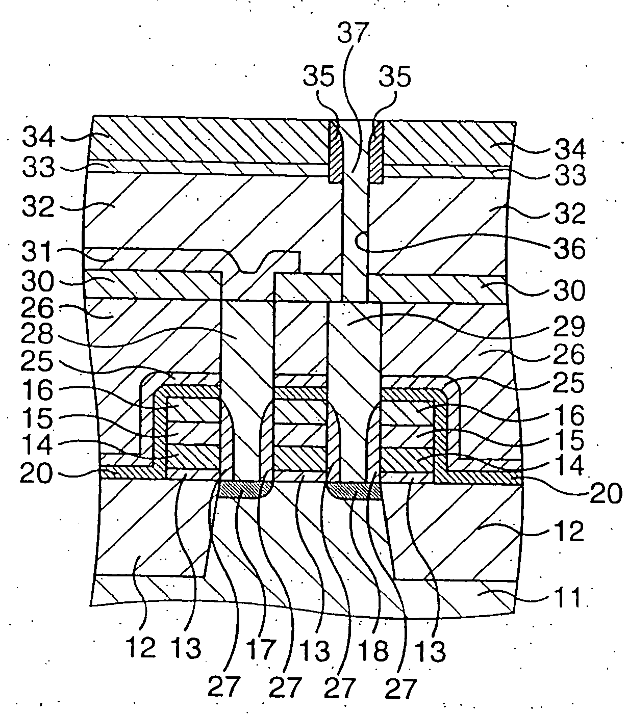
[0112] At first, fundamental features of the present invention will be briefly described with reference to FIGS. 16A and 16B.

[0113] (1) A semiconductor device according to an aspect of the present invention comprises a first insulating film 2 formed over a semiconductor substrate 1, a second insulating film 3 formed on the first insulating film 2, a contact plug 5 made of a conductive material which vertically penetrates the first and second insulating films 2 and 3 and extends on the second insulating film 3, and a conductive film in contact with the upper surface of the contact plug 5 and part of the second insulating film 3.

[0114] In this manner, the contact plug 5 is made of a conductive material which vertically penetrates the first and second insulating films 2 and 3 and extends on the second insulating film 3. With this construction, The conductive film can be brought into close contact with the contact plug 5 in a three-dimensional manner. Besides, a large contact area bet...


PUM


Abstract

A semiconductor device comprises a first insulating film formed over a semiconductor substrate, a second insulating film formed on the first insulating film, a contact plug made of a conductive material vertically penetrating the first and second insulating films and extending on the second insulating film, and a conductor film in contact with the upper surface of the contact plug and part of the second insulating film. This construction makes it possible to form minute via-holes in a mass-production line without increasing parasitic capacity, increasing the number of manufacturing steps, and generating defects.

Description

BACKGROUND OF THE INVENTION [0001] 1. Field of the Invention [0002] The present invention relates to a semiconductor device and a manufacturing method thereof, in particular, characterized by a stack structure of insulating layers which permits formation of minute via-holes without defects through a low-temperature process in a semiconductor highly-integrated circuit device such as a hybrid system LSI including a DRAM (Dynamic Random Access Memory). [0003] 2. Description of the Related Art [0004] In recent progress of integration of semiconductor integrated circuit devices, SAC (Self-Align Contact) method, MDC (Modified Contact) method, PSC (Poly Shrink Contact) method, etc., are known for forming a minute via-hole in the manner that an opening portion is formed in an insulating layer interposed between interconnection layers. These methods of forming via-holes will be described below with reference to FIGS. 1A through 1C to FIGS. 4A through 4C. [0005] First, a conventional SAC proc...

Claims


Application Information

Patent Timeline
IPC IPC(8): H01L29/94H01L21/4763H01L21/302H01L21/02H01L21/3065H01L21/316H01L21/318H01L21/60H01L21/768H01L21/8242H01L27/108
CPCG03F9/7076H01L21/28518H01L2924/0002H01L21/76816H01L21/76831H01L21/76885H01L21/76897H01L23/544H01L27/10814H01L27/10855H01L27/10888H01L27/10894H01L28/90H01L2223/5448H01L2924/00H10B12/315H10B12/0335H10B12/485H10B12/09H10B12/00
Inventor ANEZAKI, TORUIKEMASU, SHINICHIROH
Owner FUJITSU SEMICON LTD
Why Eureka
Try Eureka