Method of manufacturing electron emission source

a technology of electron emission source and emission type, which is applied in the manufacture of electrode systems, electric discharge tubes/lamps, nanoinformatics, etc., can solve the problems of difficult to control the shape of the opening in the insulating layer, damage to the exposed surface and affecting the electron emission performance of the carbon nanotube layer

Inactive Publication Date: 2006-11-16
MITSUBISHI ELECTRIC CORP
View PDF10 Cites 7 Cited by
  • Summary
  • Abstract
  • Description
  • Claims
  • Application Information

AI Technical Summary

Benefits of technology

[0008] An object of the present invention is to provide a method of manufacturing an electron

Problems solved by technology

Consequently, the exposed surface of the carbon nanotube layer is damaged.
In addition, unnecessary deposits adhere to the exposed surface of the carbon nanotube layer as well as to an inner side surface of the opening in the insulating layer.
On the other hand, according to a technique to form the opening in the insulating layer using wet etching, it is difficult to control a shape of the opening in the insulating layer.
For the reasons as described above, the conventional methods of manufacturing the electron emission source are disadvantageous in their inability to improve electron emission performance of the carbon nanotube layer.
This is

Method used


Image

  • Method of manufacturing electron emission source
  • Method of manufacturing electron emission source
  • Method of manufacturing electron emission source

Examples


first embodiment

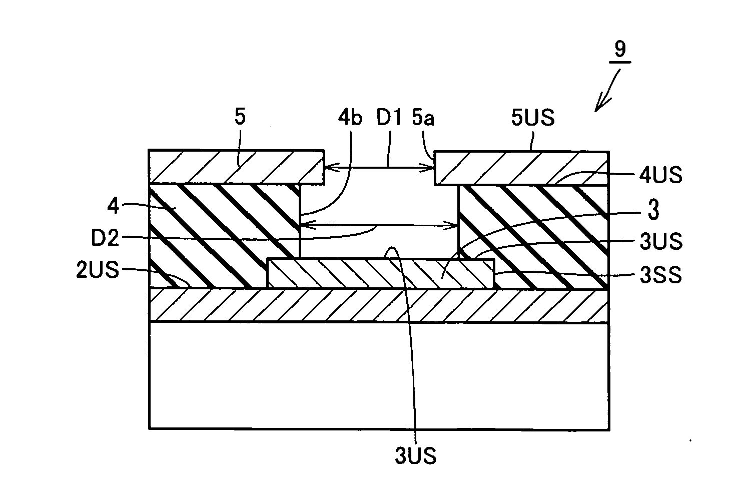
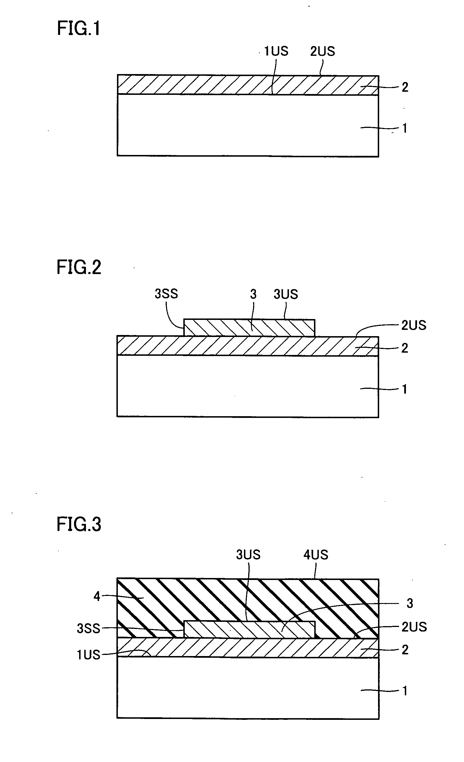
[0025] The step of manufacturing an electron emission source used in an FED back panel according to the present embodiment will initially be described with reference to FIGS. 1 to 10.

[0026]1: Formation of Cathode Electrode 2 (See FIG. 1)>

[0027] Initially, a cathode electrode 2 is formed on an upper surface 1US of a glass substrate 1, using sputtering. Cathode electrode 2 is implemented, for example, by an ITO film which is a transparent conductive film. For example, the ITO film has a film thickness of 0.3 μm.

[0028] Thereafter, cathode electrode 2 is processed to have a linear shape using photolithography or the like. Here, photolithography refers to a photomechanical process using light, electron beam or the like to transfer a pattern onto a planar substrate in a semiconductor manufacturing technology. Though various steps such as application, exposure, etching, removal, and the like of a resist film are carried out in this process, these steps are common and detailed description...

second embodiment

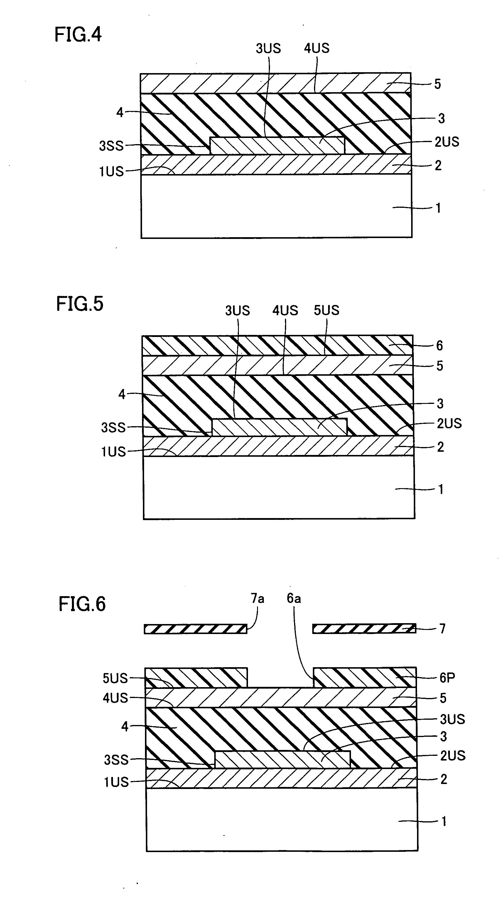
[0082] According to the first embodiment, after the second dry etching step, the exposed surface of the carbon nanotube layer is irradiated with the laser beam to improve the electron emission performance of the carbon nanotube layer. Instead of irradiation with the laser beam, as shown in FIG. 11, an adhesive 10 and an adhesive tape base material 11 may be used to peel off a surface layer portion of carbon nanotube layer 3 so that the carbon nanotubes are raised, thus improving the electron emission performance of carbon nanotube layer 3. Here, adhesive 10 and adhesive tape base material 11 are shown as examples of an adhesive material, and an adhesive material other than the tape may be employed.

[0083] Adhesive 10 has a thickness of approximately 50 μm. Adhesive 10 along with adhesive tape base material 11 is adhered to an upper surface 5US of gate electrode 5, and adhesive 10 is pressed into openings 5a and 4b with an appropriate pressure, so that adhesive 10 reaches the bottom ...

third embodiment

[0085] The first and second embodiments provide, as one example, a method of forming insulating layer 4 by using a table coater to apply PPSQ onto glass substrate 1 and subjecting PPSQ to heat treatment. In the present embodiment, instead of the method described above, a spin coater is used, that is, a spin coating method is used, to apply the varnish PPSQ solution onto glass substrate 1.

[0086] It is noted that the screen printing method may be used to apply the varnish PPSQ solution onto glass substrate 1, instead of the spin coating method. In any case, the step of drying PPSQ and subjecting the same to heat treatment in order to form insulating layer 4 is performed in a manner the same as in the first and second embodiments. When the screen printing method is employed as well, insulating layer 4 can have a thickness necessary for ensuring the withstand voltage, while an amount of varnish to be applied during squeezing is controlled to avoid unevenness caused by difference in hei...


PUM

PropertyMeasurementUnit
Pressureaaaaaaaaaa
Pressureaaaaaaaaaa
Surface energyaaaaaaaaaa

Abstract

The step of forming an opening in an insulating layer to expose a carbon nanotube layer is performed using two types of dry etching different from each other in conditions. In the first-stage dry etching step, a hole is formed in the insulating layer to such a depth as not exposing the carbon nanotube layer. Thereafter, in the second-stage dry etching step, a bottom surface portion of the hole is removed, thus exposing an upper surface of the carbon nanotube layer. A method of manufacturing an electron emission source capable of improving performance of an electron emission portion is thus obtained.

Description

BACKGROUND OF THE INVENTION [0001] 1. Field of the Invention [0002] The present invention relates to a method of manufacturing a field-emission-type electron emission source using a carbon nanotube layer as an electron emission portion. [0003] 2. Description of the Background Art [0004] An electron emission source for FED (Field Emission Display) has conventionally been manufactured. In the method of manufacturing the electron emission source, initially, a cathode electrode is formed on a substrate. Then, a carbon nanotube layer serving as an electron emission portion is formed on the cathode electrode. Thereafter, an insulating layer is formed to cover an exposed surface of the cathode electrode and an exposed surface of the carbon nanotube layer, and a gate electrode is formed on the insulating layer. Thereafter, an opening is formed in the gate electrode, and an opening is formed in the insulating layer under the opening in the gate electrode. An upper surface of the carbon nanot...

Claims


Application Information

Patent Timeline
IPC IPC(8): H01J9/04
CPCB82Y10/00H01J2201/30469H01J31/127H01J9/025H01J1/304
Inventor NISHIMURA, KUNIHIKOYASUDA, NAOKISUZUKI, YOSUKEHIROKADO, YOSHINOBUKAWAMOTO, SATORU
Owner MITSUBISHI ELECTRIC CORP
Why Eureka
Try Eureka