

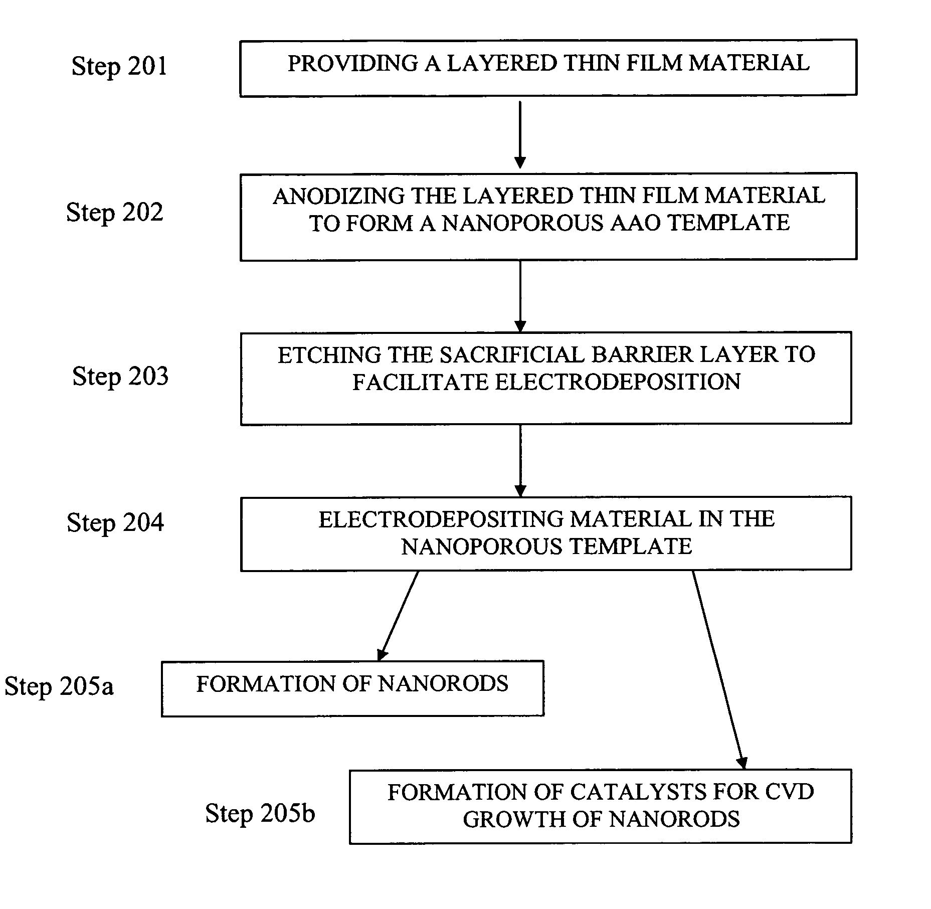
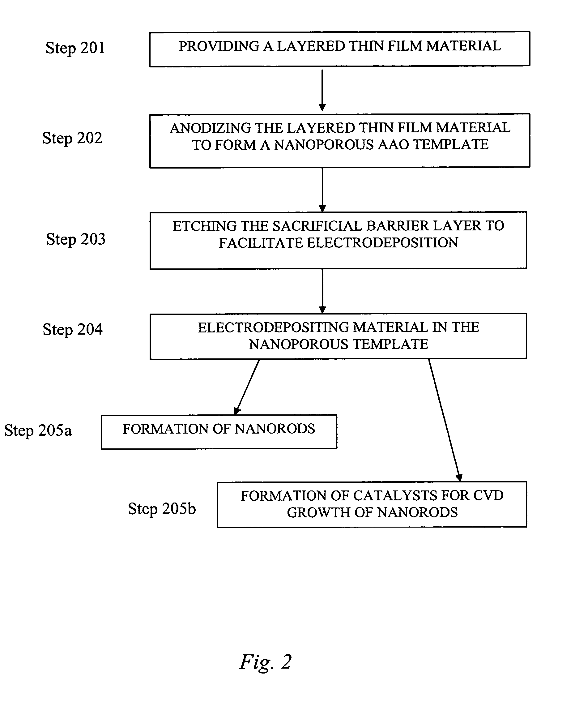
Anodized aluminum oxide nanoporous template and associated method of fabrication
an anodized aluminum oxide and nanopore template technology, applied in the field of nanopore template, can solve the problems of difficult electrodeposition of nanorods in these aao nanopore template, and the procedure is not optimal,
- Summary
- Abstract
- Description
- Claims
- Application Information
AI Technical Summary
Benefits of technology
Problems solved by technology
Method used
Image

Examples
example 1
[0045] This Example serves to illustrate the anodization of aluminum metal to AAO, in accordance with embodiments of the present invention.
[0046] In a typical anodization, a 1 micrometer thick layer of Al was deposited onto the substrate by either sputtering or electron-beam evaporation. The Al-coated substrate was used as the anode in an electrochemical cell machined from polycarbonate. Approximately 12 mm distant from the Al-coated substrate, a 25×25 mm Pt-wire gauze (Alfa) was used as the counterelectrode. The electrochemical cell was filled with a solution of 0.3 Molar oxalic acid (C2H2O4). Using a standard laboratory power supply (Agilent E3634A, 0-50 VDC, 0-4 A), the Al thin film was anodized at 25° C. for approximately 600 seconds with a constant voltage of 40 VDC and a current of about 8-12 mA / cm2. After the anodization was complete (i.e., Al completely converted to AAO), the current drops to <0.001 mA / cm . The nanoporosity may then be studied by scanning electron microscop...
example 2
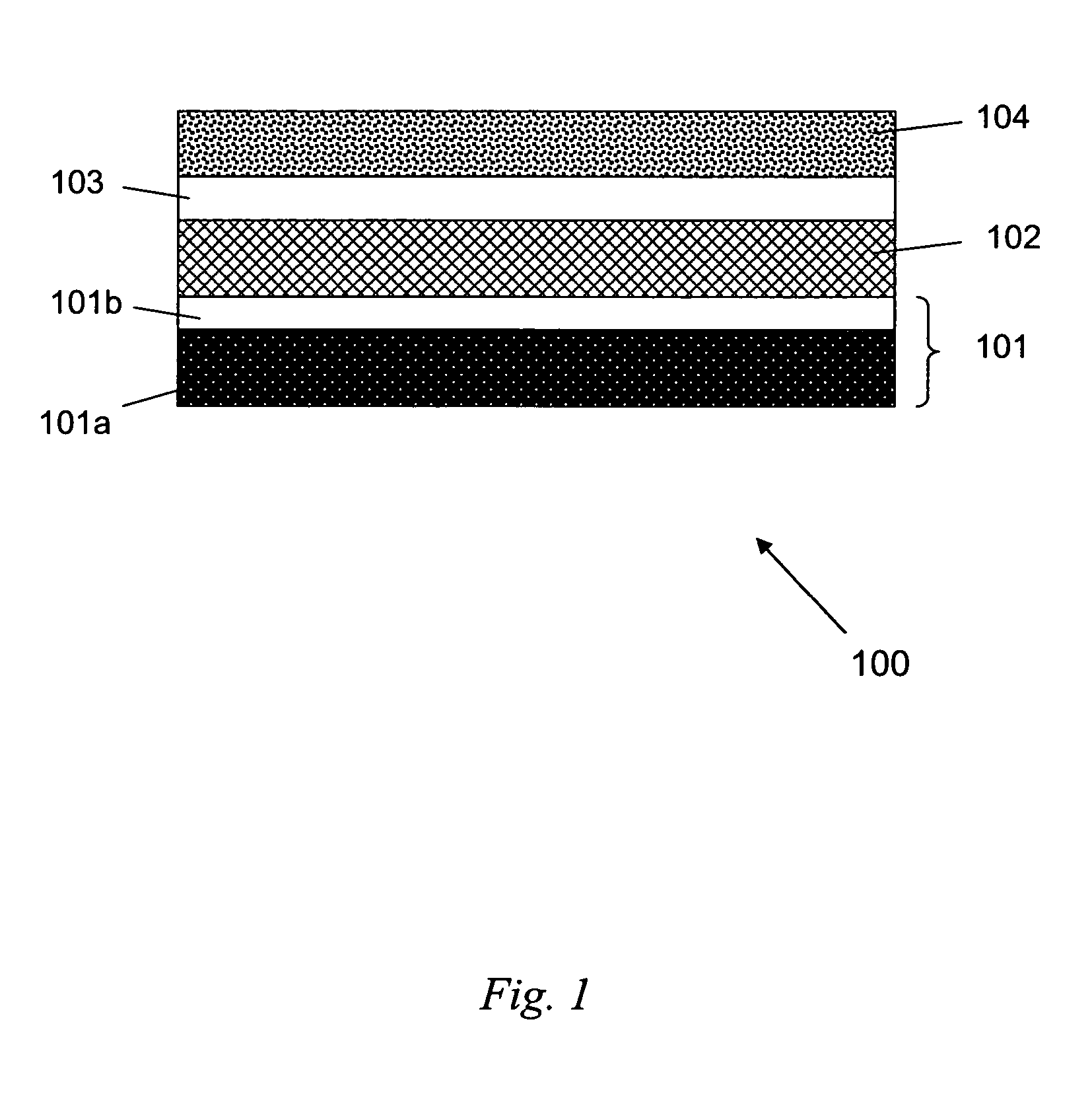
[0048] This Example serves to illustrate the anodization of layered thin film materials (i.e., several), along with their subsequent etching, to yield nanoporous AAO templates, in accordance with embodiments of the present invention.
[0049] Cleanroom produced wafers comprising a Si wafer base, a 20 nm Ti adhesion layer, a 50 nm Au (first metal) layer, a Ti (second metal) layer, and a 1000 nm Al layer. Wafers were produced having a Ti second metal layer thicknesses of 5, 10, 15, and 20 nm. Such wafers are denoted Si-wafer / 20 nm Ti / 50 nm Au / x nm Ti / 1000 nm Al, where x is 5, 10, 15, and 20 nm. For each wafer, the Al was anodized until an insulating sacrificial barrier layer of TiOx was formed (the exact stoichiometry of the anodized Ti is unknown at present). As it is known that TiO2 is etched by a solution of 20 H2O:1 HF:1 H2O2 (by volume) at a rate of 880 nm / minute (Williams et al., J. MEMS 1996, 5 (4), p. 256; Williams et al., J. MEMS 2003, 12 (6), p. 761), the anodized wafers were ...
example 3
[0050] This Example serves to illustrate the subsequent electrodeposition of Pt into nanopores of a nanoporous AAO template to form Pt nanorods.
[0051] Cyclic voltammetry and Pt nanorod electrodeposition were used to characterize etched wafer samples and provide large area nanoporous AAO templates (0.75 inches in diameter), uniformly filled with Pt nanorods. The electrochemical procedures used a commercially-available 10 grams / gallon platinum plating solution (Technic, Inc., Cranston, R.I., product no. #240651); a layered thin film material denoted Si wafer / 20 nm Ti / 50 nm Au / 10 nm TiOx / 1200 nm AAO, and comprising a Si-wafer base (2.5 cm in diameter), a 20 nm Ti adhesion layer, a 50 nm Au (first metal layer), a 10 nm TiOx sacrificial barrier layer, and a 1200 nm AAO layer, wherein the layered thin film material serves as the working electrode; a 25×25 mm Pt wire gauze, 45 mesh, woven from 0.198 mm diameter wire (Alfa Aesar, stock #41814) serves as the counter electrode; and a Ag / AgCl...
PUM
| Property | Measurement | Unit |
|---|---|---|
| Fraction | aaaaa | aaaaa |
| Fraction | aaaaa | aaaaa |
| Diameter | aaaaa | aaaaa |
Abstract
Description
Claims
Application Information