
Process and apparatus for producing single crystal

a technology of process and apparatus, applied in the direction of single crystal growth, electrical apparatus, chemistry apparatus and processes, etc., can solve the problems of low single crystal growth rate, disadvantageous heating of reactor per se, and inability to grow single crystals without difficulties, etc., to achieve high efficiency, easy temperature control, and uniform thickness

Inactive Publication Date: 2007-01-25
CRYSTAL SYST
View PDF1 Cites 13 Cited by
  • Summary
  • Abstract
  • Description
  • Claims
  • Application Information

AI Technical Summary

Benefits of technology

[0014] Accordingly, an object of the present invention is to provide a process for producing a single crystal by chemical vapor deposition, which can produce a high-quality thick single crystal film without wasteful consumption of a raw material gas while suppressing bending and the like.
[0016] The present inventors have made extensive and intensive studies with a view to solving the above problems of the prior art and as a result have found that, when a production process of a single crystal comprising producing a single crystal on a colored substrate by chemical vapor deposition and characterized by focusing infrared light with a reflecting mirror to directly heat both sides of the colored substrate is used, only the crystal growth surface on the substrate can be heated and maintained at a desired temperature and, in addition, temperature conditions for providing a very homogeneous temperature with a very small temperature distribution can be realized on the substrate and that, thus, the raw material gas can be efficiently used and a high-quality single crystal in which the level of defect is very small can be produced with high efficiency. The present inventors have further found that a single crystal can be efficiently produced by allowing the single crystal to grow on both sides of the substrate, and, at the same time, the occurrence of bending attributable to a difference in coefficient of thermal expansion during cooling can be reduced and the substrate and the grown high-quality single crystal can be easily isolated from each other by simple cutting. The above finding has led to the completion of the present invention.
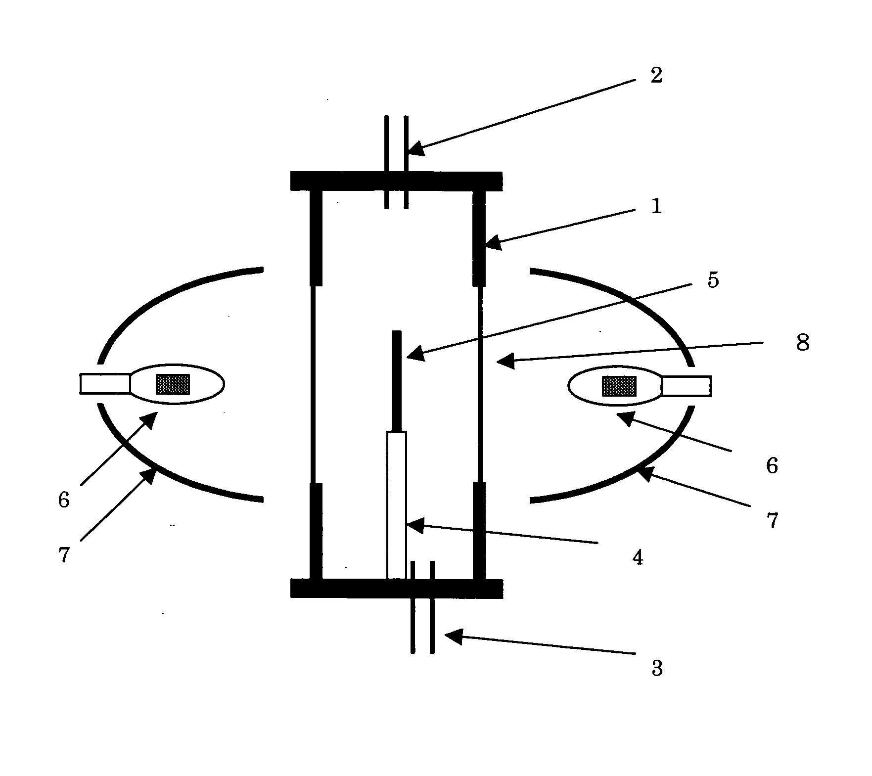
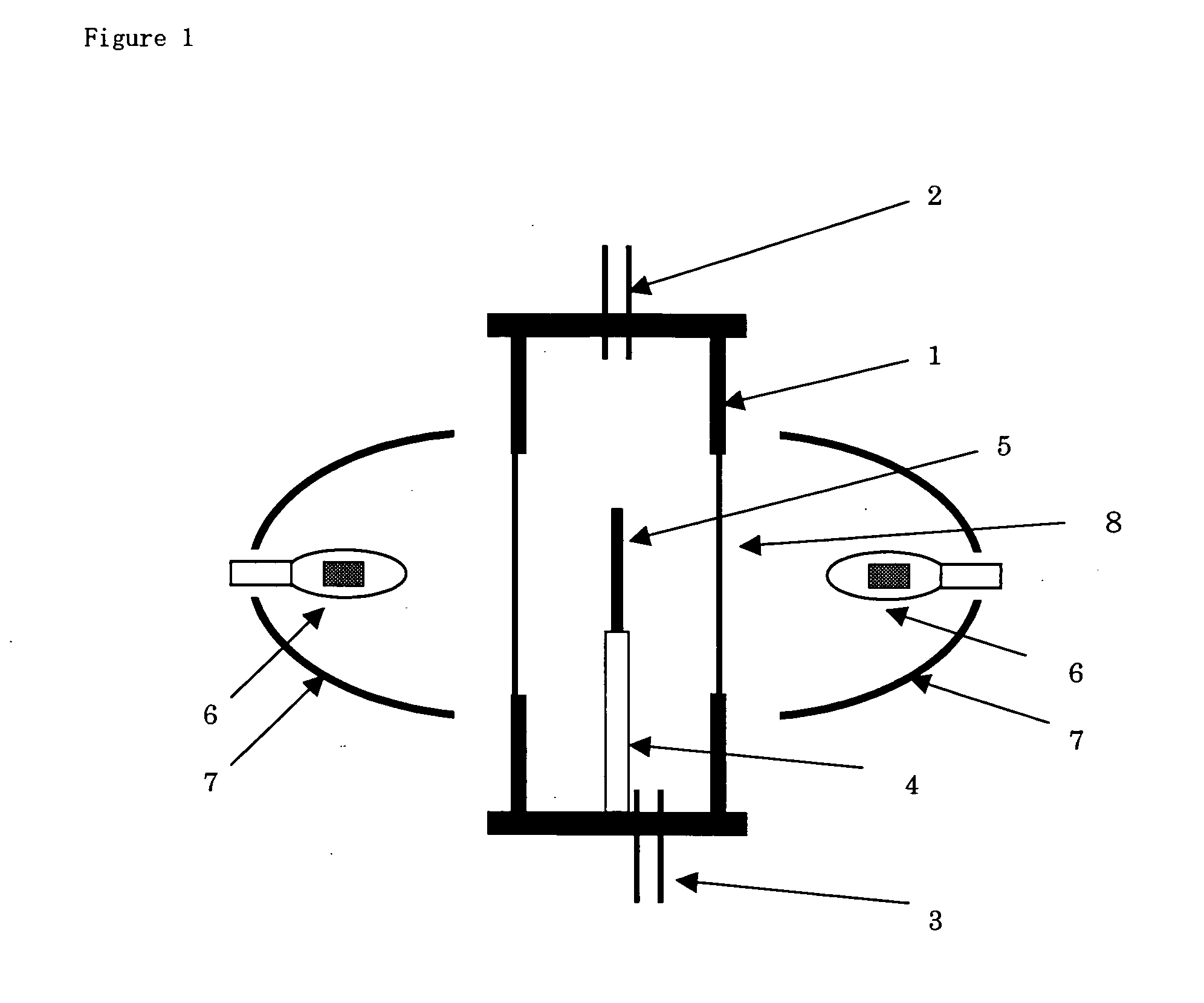
[0020] According to another aspect of the present invention, there is provided an apparatus for producing a single crystal on both sides of a colored substrate, said apparatus comprising a reactor and at least a pair of infrared irradiation devices each comprising an infrared generating source and a reflecting mirror, wherein said colored substrate is fixed through a substrate holder within said reactor, said reactor comprises a raw material gas introduction tube, a waste gas discharge tube, and an infrared transparent window, said at least one pair of infrared irradiation devices are disposed outside said reactor so as to face each other, and both sides of said colored substrate on which said single crystal is grown are substantially evenly heated by said infrared irradiation devices through said infrared transparent window.
[0022] In the production process of a single crystal according to the present invention, only the colored substrate can be selectively heated, and, further, the temperature control can also be easily carried out. Therefore, a single crystal can be produced with a significantly high efficiency. Furthermore, a single crystal, which has uniform thickness and is free from a significant level of bending, can be produced simultaneously on both sides of the substrate so as to sandwich the substrate therebetween. At the same time, a thick bulk single crystal can also be easily produced.

Problems solved by technology

On the other hand, for nitride semiconductors comprising nitrogen (N) as a constituent element among compound semiconductors, the equilibrium vapor pressure of nitrogen at the melting point of the crystal is so high that a single crystal cannot be grown by the above HB and LEC methods without difficulties.
The conventional method, however, suffers from a problem that the growth rate of the single crystal is low and is about several microns per hr.
In the method in which the whole reaction chamber is heated, however, the reactor per se is also disadvantageously heated.
Therefore, the reaction proceeds in the whole reactor, and, in many cases, selective growth of a thin film single crystal on a substrate has been difficult.
Further, due to the restriction of the softening temperature of quartz (about 1200° C.) commonly used as the reactor vessel, the growth of the single crystal at a temperature at or above this temperature has been difficult.
In the method (i) in which a resistance heating type heater is used, however, for example, a raw material gas comprising an organometal gas, hydrogen chloride gas and the like or an exhaust gas after the completion of the reaction is in some cases very highly reactive and is highly corrosive, often making it difficult to stably use the heater for a long period of time due to the corrosion of the heater.
Further, in the method (ii) in which the substrate is heated by the high frequency dielectric heating method and the method (iii) in which a plate formed of a material capable of absorbing infrared light such as graphite (hereinafter referred to as “substrate plate”) is placed on the lower side of the substrate to heat the substrate indirectly, the susceptor or the substrate plate becomes the highest temperature and, in addition, the temperature of a part around the susceptor and the substrate plate is also raised, thus, disadvantageously, the reaction also takes place on the periphery of the substrate around the substrate plate.
Accordingly, the expensive raw material gas is wastefully consumed, and these methods cannot solve the problem that stable growth of a single crystal on the substrate is inhibited.
This makes it difficult to lower the temperature after the completion of the growth reaction for isolating the substrate and the single crystal from each other, and, thus, in some cases, renders the occurrence of cracks and the like during the isolation work unavoidable.
This process, however, is disadvantageous in that, due to bending after the growth of the single crystal, simple cutting work cannot be applied without difficulties in the process of isolating the thin film single crystal from the substrate and, thus, the isolation should be carried out by a special method such as laser beam irradiation.
In the cutting process, in some cases, cracking or the like disadvantageously takes place, and, thus, there is still a problem to be solved for stably producing a high-quality thick single crystal film.

Method used


Image

  • Process and apparatus for producing single crystal
  • Process and apparatus for producing single crystal

Examples


example 1

[0089]

[0090] For example, an apparatus exemplified in FIG. 1 may be mentioned as an embodiment of a single crystal production apparatus for use in the production process of the present invention.

[0091] In this apparatus for producing a thin-film single crystal, a reactor (1), which is provided with a raw material gas introducing tube (2) and a discharge tube (3) for discharging a waste gas and has an infrared transparent window (8), is provided. A colored substrate (5) is fixed substantially vertically through a substrate holder (4) within the reactor (1). A set of infrared irradiation devices each comprised of an infrared generating source (6) and a reflecting mirror (7) are disposed outside the reactor (1).

[0092] A transparent quartz plate is used as a window material in the reactor (1), and a single crystal plate of ruby as the colored substrate (5). The infrared generating source (6) is a halogen lamp. An elliptical mirror is used in the reflecting mirror (7). When the reflect...

example 2

[0098]

[0099] An aluminum nitride single crystal was produced using the single crystal production apparatus used in Example 1.

[0100] At the outset, aluminum trichloride was filled into a separately provided thermostatic vessel. This vessel was then maintained at a constant temperature of 100 to 150° C., and hydrogen gas was passed through the vessel to introduce aluminum trichloride vapor corresponding to the temperature through the raw material gas introducing tube (2) into the reactor (1). Likewise, ammonia gas, together with hydrogen gas as carrier gas, was introduced through the raw material gas introducing tube (2) into the reactor (1). The ruby single crystal plate was heated to 1350° C. by infrared light which had been emitted from the halogen lamp and focused by the elliptical mirror, and, while maintaining the temperature of the ruby single crystal plate at that temperature, a single crystal of gallium nitride was grown on both sides of the ruby single crystal plate. As a r...


PUM


Abstract

Disclosed are a production apparatus and a production process in which a thick and high-quality single crystal film can be formed on both sides of a colored substrate. Both single crystal growth surfaces of a colored substrate which has been fixed through a substrate holder within a reactor are substantially evenly heated by at least one pair of infrared irradiation devices each comprising an infrared generating source and a reflecting mirror to produce a single crystal.

Description

FIELD OF THE INVENTION [0001] The present invention relates to a process and apparatus for producing a single crystal. More particularly, the present invention relates to a process and apparatus for producing a high-quality single crystal which is suitable for use as a fundamental element of a semiconductor element used in a wide variety of equipment such as laser equipment and optical communication equipment. BACKGROUND OF THE INVENTION [0002] Single crystals have hitherto been widely used as fundamental elements indispensable to semiconductor elements for use in a wide variety of equipment such as laser equipment and optical communication equipment, specifically as substrate wafers. In particular, for example, an HB (horizontal Bridgman) method and an LEC (liquid encapsulated Czochralski) method have been used as a production process of a single crystal of a compound semiconductor for use in optical elements to put compound semiconductors such as GaAs, InP, GaP, and InAs to practi...

Claims


Application Information

Patent Timeline
IPC IPC(8): H01L21/76
CPCC30B29/40C30B25/105
Inventor SHINDO, ISAMUKOUKITU, AKINORI
Owner CRYSTAL SYST
Learn More