Production method of gallium nitride-based compound semiconductor multilayer structure
- Summary
- Abstract
- Description
- Claims
- Application Information
AI Technical Summary
Benefits of technology
Problems solved by technology
Method used
Image

Examples
example 1
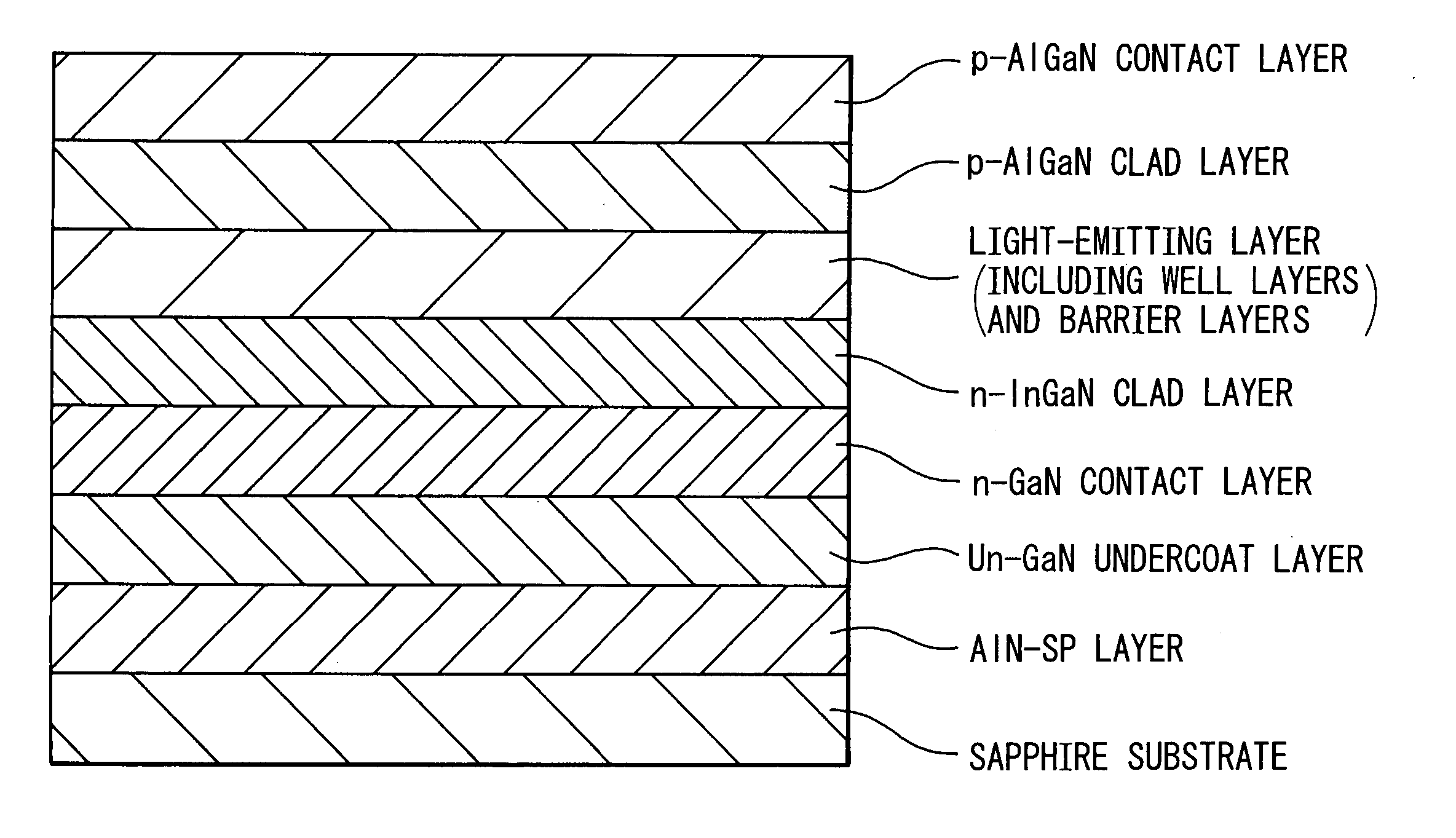
[0118]FIG. 1 schematically shows a gallium nitride-based compound semiconductor multilayer structure, for producing a semiconductor light-emitting device, which was fabricated as Example 1 (configuration of well layers and barrier layers in the light-emitting layer being omitted). As shown in FIG. 1, an SP layer formed of AlN is stacked on a sapphire substrate having a c-plane through a lattice-mismatch crystal epitaxial growth method. On the SP layer, the following layers are sequentially formed: an undoped GaN undercoat layer (thickness: 8 μm); a highly-Ge-doped GaN contact layer (electron concentration: 1×1019 cm−3, thickness: 2 μm); an Si-doped In0.02Ga0.98N clad layer (electron concentration: 1×1018 cm−3, thickness: 20 nm); a light-emitting layer of a multiple quantum well structure including 6 Si-doped GaN barrier layers (electron concentration: 3×1017 cm−3, thickness of each layer: 15 nm) and 5 undoped In0.08Ga0.92N well layers (thickness of each layer: 3 nm); an Mg-doped p-t...
example 14
[0165]FIG. 1 schematically shows a gallium nitride-based compound semiconductor multilayer structure for producing a semiconductor light-emitting device of which the structure was fabricated as this Example (configuration of well layers and barrier layers in the light-emitting layer being omitted). As shown in FIG. 1, an SP layer formed of AlN is stacked on a sapphire substrate having a c-plane through a lattice-mismatch crystal epitaxial growth method. On the SP layer, the following layers are sequentially formed: an undoped GaN undercoat layer (thickness: 8 μm); a highly-Ge-doped GaN contact layer (electron concentration: 1×1019 cm−3, thickness: 2 μm); an Si-doped In0.02Ga0.98N clad layer (electron concentration: 1×1018 cm−3, thickness: 20 nm); a light-emitting layer of a multiple quantum well structure including 6 Si-doped GaN barrier layers (electron concentration: 3×1017 cm−3, thickness of each layer: 15 nm) and 5 undoped In0.08Ga0.92N well layers (thickness of each layer: 3 nm...
example 15
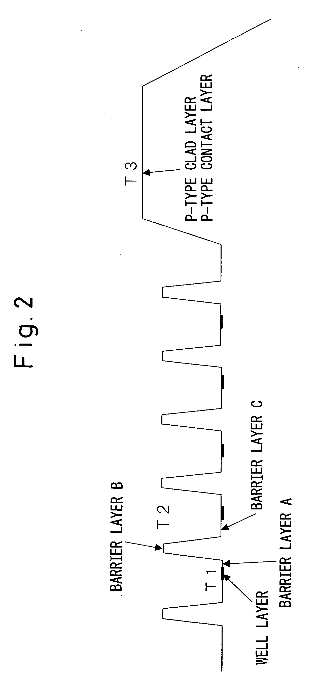
[0200] Light-emitting diodes were produced in the same manner as in Example 14 except for changing the supply amount of TEGa so that the growth rates of Si-doped GaN barrier layer A and B were 3 Å / min and the growth rate of Si-doped GaN barrier layer C was 7 Å / min, and the obtained light-emitting diode was evaluated in the same manner as in Example 14.
[0201] The diode exhibited a forward voltage (an operating voltage) of 3.3 V at a current of 20 mA, an emission wavelength of 460 nm, and a light emission output of 5.5 mW. Such characteristics of the light-emitting diode can be attained without variation among light-emitting diodes cut and produced from virtually the entirety of the above-fabricated gallium nitride-based compound semiconductor multilayer structure.
[0202] A current of 30 mA was passed through this light-emitting diode in the forward direction and when an aging test of measuring the light emission output at the start and after 100 hours was performed and the degradati...
PUM
 Abstract
Description
Claims
Application Information
 - Generate Ideas
- Intellectual Property
- Life Sciences
- Materials
- Tech Scout
- Unparalleled Data Quality
- Higher Quality Content
- 60% Fewer Hallucinations
Browse by: Latest US Patents, China's latest patents, Technical Efficacy Thesaurus, Application Domain, Technology Topic, Popular Technical Reports.
© 2025 PatSnap. All rights reserved.Legal|Privacy policy|Modern Slavery Act Transparency Statement|Sitemap|About US| Contact US: help@patsnap.com