
Method and structure for fabricating non volatile memory arrays

Active Publication Date: 2007-02-01
WINBOND ELECTRONICS CORP
View PDF2 Cites 6 Cited by
  • Summary
  • Abstract
  • Description
  • Claims
  • Application Information

AI Technical Summary

Benefits of technology

[0007] According to the present invention, techniques for fabricating integrated circuit devices are provided. More particularly, the invention provides a method and structure for a non-volatile memory device, commonly called a metal oxide-nitride-oxide on silicon (“MONOS”) memory device. Merely by way of example, the present invention provides a method for processing a cell region of the MONOS memory separately while protecting peripheral regions of the device for efficiency and improvement in device characterization. The peripheral regions are then processed while protecting the cell region in other embodiments. Certain steps are performed to process both the peripheral and cell region for efficiency and improved process integration purposes.
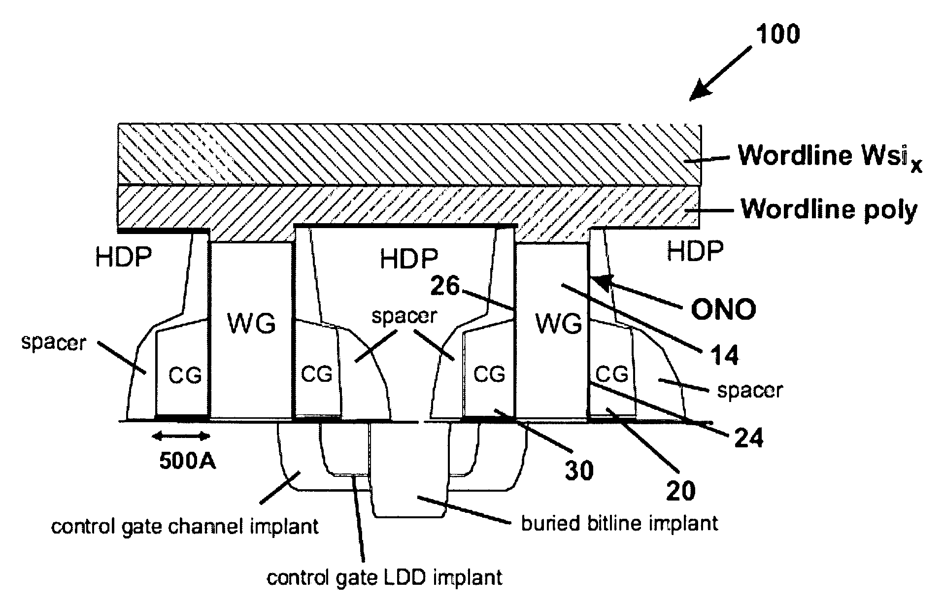
[0013] (1) A fabrication process that forms memory cell array first, while peripheral poly is protected by an oxide layer to protect peripheral poly from later word line (WL) etch. After word gate (WG) deposition in our present flow, cap oxide is used to protect peripheral poly against a later WL etch, which stops on oxide. In the memory cell area, however, oxide is removed by a cell mask. The word gate is thereafter formed after SiN layer is deposited. As mentioned before, during WG etch, the peripheral poly is protected. Such a memory first process provides an ability to develop and possibly optimize the memory cells first without affecting peripheral logic transistor architecture.
[0014] (2) The buried bit line (BL) formation uses a high density plasma (HDP) oxide layer, and includes a reverse mask to remove oxide on peripheral region, which has logic circuitry. After WG formation, while peripheral poly has been protected, many processes including control gate (CG) channel implant, oxide-on-nitride (ONO) / CG poly deposit and etch, cell LDD, oxide spacer, and BL implant are provided to make a functional memory cell transistor. Afterward, oxide-fill in-between BLs is provided for isolation. As device dimension shrinks, a gap fill oxide deposition process is needed to fill the narrow BL spacing. Preferably, high density plasma oxide has been used. A reverse mask is then employed to clear peripheral area oxide first before BL oxidation oxide chemical mechanical polishing, commonly called CMP. Such approach provides an advantage of shorter process time, better process control, and wider process window, among other possible benefits. Chemical Mechanical Polishing technology has certain oxide to SiN selectivity such that minor surface morphology (i.e., shallow trench isolation (STI) edge) may pose a problem for complete oxide removal without additional wet process after CMP. By using this embodiment of the invention, the additional wet recess process after the word gate, CMP could be used to optimize BL oxide recess specifically. Such BL oxide recess is often important or even critical for preventing shortage between nodes (e.g., WL, CG, WG).
[0015] (3) Simultaneous contact formation for WL, buried BL, logic gate and logic S / D. A practical manufacturing contact scheme is often a challenge for the buried diffusion BL cell architecture, since BL has been sealed by HDP oxide in a relatively early stage of the process and a relatively high contact aspect ratio. According to a preferred embodiment of the present invention, we adopted the scheme to form four different contacts simultaneously, with a single step. As shown below, four contacts includes WL (with biggest step high ), BL contact, logic gate contact, and logic S / D contact( with deepest aspect ration (A.R.)). Simultaneous contact formation often saves process steps and mask counts according to preferred embodiments.
[0016] As noted, numerous benefits may be achieved using the present invention over other techniques. For example, the present invention provides an efficient way to optimize the cell region structures independently from the peripheral region structures. The cell region structures will include the MONOS memory devices. The peripheral region structures will include logic transistors. In other embodiments, the invention may use convention process technology for efficiency and reliability. One or more of these benefits may be achieved depending upon the embodiment. These and other benefits are described throughout the present specification and more particularly below.

Problems solved by technology

Fabrication of this type of MONOS device has many challenges, such as spacer etch to form the control gates, diffusion bit line isolation, contact formation, word line formation, and integration of the cell area and the peripheral area, etc.

Method used


Image

  • Method and structure for fabricating non volatile memory arrays
  • Method and structure for fabricating non volatile memory arrays
  • Method and structure for fabricating non volatile memory arrays

Examples


Embodiment Construction

[0021] According to the present invention, techniques for fabricating integrated circuit devices are provided. More particularly, the invention provides a method and structure for a non-volatile memory device, commonly called a metal oxide-nitride-oxide on silicon (“MONOS”) memory device. Merely by way of example, the present invention provides a method for processing a cell region of the MONOS memory separately while protecting peripheral regions of the device for efficiency and improvement in device characterization. The peripheral regions are then processed while protecting the cell region in other embodiments. Certain steps are performed to process both the peripheral and cell region for efficiency and improved process integration purposes.

[0022] Depending upon the embodiment, the present invention includes various features, which may be used. These features include the following:

[0023] 1. Buried BL formation including using an HDP oxide layer and using a reverse mask to remov...


PUM


Abstract

An MONOS integrated circuit device. The device has a semiconductor substrate comprising a silicon bearing material and a shallow trench isolation region formed within the substrate. A P-type well region is formed within the substrate and adjacent to the shallow trench isolation region. The first word gate comprising a first edge and a second edge. The first word gate comprises a first control gate coupled to the first edge and a second control gate coupled to the second edge. Preferably, the second word gate comprises a first edge and a second edge. The second word gate comprises a first control gate coupled to the first edge and a second control gate coupled to the second edge. A common buried bit line is formed within the P-type well region and between the second edge of the first word gate and the first edge of the second word gate. An HDP plasma dielectric is formed overlying the common buried bitline to a height within a vicinity of a first surface of the first word gate and a second surface of the second word gate. In a preferred embodiment, the device has a planarized surface formed from a portion of the HDP plasma dielectric, the first surface, and the second surface. A word line is overlying the planarized surface. The word line is coupled to the first word gate and the second word gate and is overlying the HDP plasma dielectric. The device has a refractory metal layer formed overlying the word line, a hard mask layer overlying the refractory metal layer, and a cap layer formed overlying the hard mask layer. The word line, refractory metal layer, hard mask layer, and cap layer form a planarized structure.

Description

BACKGROUND OF THE INVENTION [0001] The present invention relates generally to integrated circuit devices. More particularly, the invention provides a method and structure for a non-volatile memory device, commonly called a metal oxide-nitride-oxide on silicon (“MONOS”) memory device. Merely by way of example, the present invention provides a method for processing a cell region of the MONOS memory separately while protecting peripheral regions of the device for efficiency and improvement in device characterization. The peripheral regions are then processed while protecting the cell region in other embodiments. Certain steps are performed to process both the peripheral and cell region for efficiency and improved process integration purposes. [0002] Integrated circuits proliferated through the years. Certain types of integrated circuits include memory devices. The memory devices include volatile memories such as dynamic random access memory devices, commonly called “DRAMs” and non-vola...

Claims


Application Information

Patent Timeline
IPC IPC(8): H01L21/336
CPCH01L27/105H01L27/11573H01L27/11568H01L27/115H10B69/00H10B43/40H10B43/30
Inventor CHOU, KAI CHENGLAUN, HARRYHUANG, KENLINYOUNG, J.C.WANG, ARTHUR
Owner WINBOND ELECTRONICS CORP
Features
  • Generate Ideas
  • Intellectual Property
  • Life Sciences
  • Materials
  • Tech Scout
  • Unparalleled Data Quality
  • Higher Quality Content
  • 60% Fewer Hallucinations
Learn More