Transparent conductive film and transparent conductive base material utilizing the same

a technology of transparent conductive base material and transparent conductive film, which is applied in the direction of conductive layers on insulating supports, non-metal conductors, instruments, etc., can solve the problems of insufficient work function and difficult control, and achieve low surface resistance and high work function.

Inactive Publication Date: 2007-03-08
SUMITOMO METAL MINING CO LTD
View PDF3 Cites 27 Cited by
  • Summary
  • Abstract
  • Description
  • Claims
  • Application Information

AI Technical Summary

Benefits of technology

[0011] The object of the present invention is to provide a transparent conductive film which combines a low surface resistance with a high work function and is laminated by transparent conductive thin films, and a transparent conductive base material using this transparent conductive film.
[0022] In particular, when the transparent conductive film is used as the anode of the organic EL element or the like, the injection of positive holes become easy. As a result, the transparent conductive film is capable of improving the light-emitting efficiency of the organic EL element and this is useful.
[0023] The transparent conductive base material of the present invention is obtained by forming the transparent conductive film of the present invention after the gas barrier film is formed, when the necessity arises, not only on a glass substrate or a quartz substrate but also on a resin substrate that has no heat resistance or a flexible resin film substrate. Hence, in any shape and contour of the device, the transparent conductive base material can be utilized as the base material of a flexible transparent organic EL element using the resin film substrate. This is extremely high in the value of industry.

Problems solved by technology

However, it is generally known that the work function of the ITO film is about 4.4 eV, and this work function is not sufficient to use the ITO film as the anode of the organic EL element.
However, the work function is highly sensitive to a processing condition and thus its control is difficult.
However, the work function of the IZO film is about 4.8-4.9 eV, which is not said to be high enough to use the IZO film as the anode of the organic EL element.

Method used


Image

  • Transparent conductive film and transparent conductive base material utilizing the same
  • Transparent conductive film and transparent conductive base material utilizing the same

Examples


embodiments

[0037] In accordance with FIGS. 1 and 2, the structures of embodiments will be described.

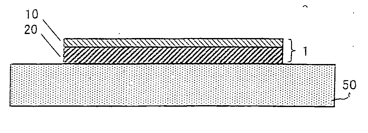
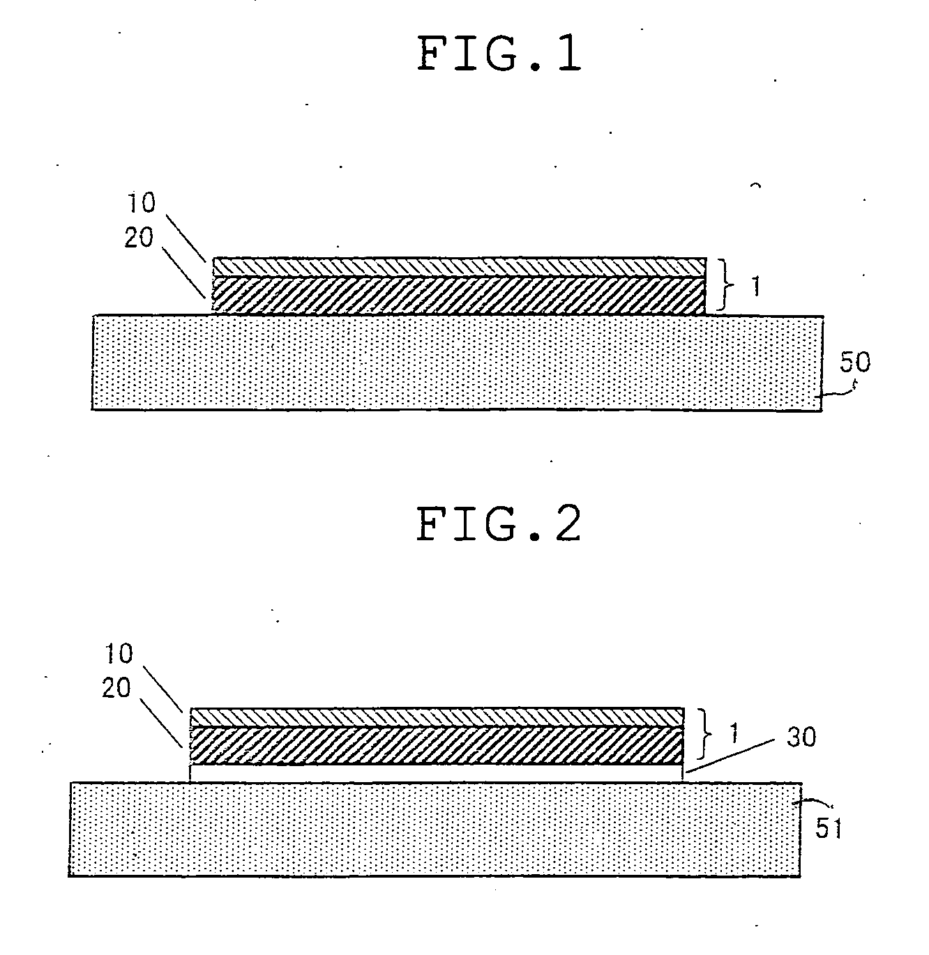
[0038]FIG. 1 is a sectional view showing the fundamental structure of the transparent conductive base material used in Embodiments 1-6. A transparent conductive film 1 is fabricated which has the lamination structure including a transparent conductive thin film 20 and a transparent conductive thin film 10 composed of gallium, indium, and oxygen, laminated in turn on a glass substrate (7059 substrate by Corning Inc.) 50. The transparent conductive thin films 10 and 20 are deposited through a direct-current magnetron sputtering method by using an SPF-530H sputtering device made by ANELVA Corporation. The transparent conductive thin films 10 and 20 are also deposited by adjusting the time so that preset film thicknesses are reached, using a gas mixture of argon and oxygen, at an output of 200 W under the conditions of a gas pressure of 0.5 Pa and a proportion of an oxygen flow rate of 1.5-2.5%.

[0...

embodiments 1-3

[0043] The transparent conductive thin film 10 is formed as an amorphous film with a thickness of 10 nm, composed of gallium, indium, and oxygen, and three kinds of compositions are provided so that gallium contents are 49.1, 50, and 65 atom %, respectively, with respect to all metallic atoms. The transparent conductive thin film 20 is formed as an In2O3-1 wt % WO3 amorphous film with a thickness of 150 nm.

[0044] As seen from Embodiments 1-3, when the gallium content of the transparent conductive thin film 10 is in the range of 49.1 to 65 atom %, the transparent conductive film 1 with a work function of 5.1 eV or more and a surface resistance of 50 Ω / □ or less can be attained.

embodiments 4-6

[0045] The transparent conductive thin film 10 is formed as an amorphous film with a thickness of 10 nm, composed of gallium, indium, and oxygen, and only one kind of composition is provided so that the gallium content is 50 atom % with respect to all metallic atoms. The transparent conductive thin film 20 is formed as one selected from among an In2O3-10 wt % SnO2 amorphous film, an In2O3-10 wt % ZnO amorphous film, and an In2O3-1 wt % WO3-0.5 wt % ZnO amorphous film, each with a thickness of 150 nm.

[0046] As seen from Embodiments 4-6, when the transparent conductive thin film 10 with a thickness of 10 nm and a gallium content of 50 atom % is combined with the transparent conductive thin film 20 formed as one selected from among the In2O3-10 wt % SnO2 amorphous film, the In2O3-10 wt % ZnO amorphous film, and the In2O3-1 wt % WO3-0.5 wt % ZnO amorphous film, each with a thickness of 150 nm, the transparent conductive film 1 with a work function of 5.1 eV or more and a surface resist...


PUM

PropertyMeasurementUnit
thicknessaaaaaaaaaa
thicknessaaaaaaaaaa
resistivityaaaaaaaaaa

Abstract

The transparent conductive film 1 includes laminated transparent conductive thin films 10 and 20 of at least two layers. The transparent conductive thin film of the uppermost layer is an amorphous oxide thin film composed of gallium, indium, and oxygen, a gallium content ranges from 49.1 atom % to 65 atom % with respect to all metallic atoms, a work function is 5.1 eV or more, and a surface resistance is 100 Ω / □ or less. The transparent conductive base material includes a transparent substrate and the transparent conductive film 1 formed one or both surfaces of the transparent substrate.

Description

TECHNICAL FIELD [0001] This invention relates to a transparent conductive film used in an organic electroluminescence (EL) element or the like and a transparent conductive base material utilizing this transparent conductive film. BACKGROUND ART [0002] The transparent conductive films have a high conductivity (for example, a resistivity of 1×10⁻³ Ω cm or less) and a high transmittance in the visible region and thus are utilized as the electrodes of solar cells, liquid crystal display elements and other various light-receiving elements, followed by heat wave reflective films used for window glass of cars and buildings, various antistatic films, and antifogging transparent heating elements for refrigerating show cases. [0003] As the transparent conductive films, antimony- or fluorine-doped tin oxide (SnO2) films, aluminum- or gallium-doped zinc oxide (ZnO) films, and tin-doped indium oxide (In2O3) films are widely utilized. In particular, the tin-doped indium oxide films, namely In2O3-...

Claims


Application Information

Patent Timeline
Patent Type & Authority Applications(United States)
IPC IPC(8): H01B1/12B32B9/00C03C17/245C03C17/34C23C14/08C23C14/34G02F1/1333G02F1/1343H01B1/08H01B5/14H05B33/28
CPCC03C17/3417C23C14/08H05B33/28G02F1/13439H01B1/08C23C14/086H01L21/20
Inventor NAKAYAMA, TOKUYUKIABE, YOSHIYUKI
Owner SUMITOMO METAL MINING CO LTD
Why Eureka
Try Eureka