Integrated process for sputter deposition of a conductive barrier layer, especially an alloy of ruthenium and tantalum, underlying copper or copper alloy seed layer

a technology of conductive barrier layer and integrated process, which is applied in the direction of resistive material coating, chemical vapor deposition coating, solid-state devices, etc., can solve the problems of loss of insulating characteristics, copper cannot directly contact the dielectric layer, and copper does not adhere well to oxide, etc., to achieve effective interfacial barrier

Inactive Publication Date: 2007-03-15
APPLIED MATERIALS INC
View PDF21 Cites 136 Cited by
  • Summary
  • Abstract
  • Description
  • Claims
  • Application Information

AI Technical Summary

Benefits of technology

[0027] Yet a further aspect of the invention includes alloying the RuTa or related barrier and adhesion layers with aluminum. When annealed, the resultant aluminum oxide acts as an interfacial barrier to moisture and other diffusing particles particularly from porous low-k dielectrics. Similar aluminum doping of ruthenium also creates an effective interfacial barrier.
[0028] One more aspect of the invention includes a contact liner structure for copper contact metallization over a silicon or silicide layer in which RuTa contact hole liners of different alloying fractions also coat the hole bottom with the respective alloying fractions selected to produce a work function better suited to the doping type of the underlying silicon layer.
[0029] A noble copper alloy seed layer may be formed of copper and one the Group VIIIB elements except iron. Ruthenium copper is the preferred noble copper alloy. The alloying percentages may be freely chosen, but small copper content below 25 at % is preferred ranging down to 1 at % or even 0.01 at %. The noble copper alloy seed layer may serve as an electroplating electrode, especially for copper.

Problems solved by technology

One challenging application in the fabrication of advanced integrated circuits is the sputter deposition of thin liner layers in vertical electrical interconnects, usually called vias, for copper metallization.
However, copper cannot directly contact the dielectric layer 86.
Copper does not adhere well to oxide.
Copper also can diffuse into the upper-level dielectric layer 86 and cause it to lose its insulating characteristics and short out the devices being formed.
As will be discussed later, the copper continuity has become a major issue.
However, future generations of integrated circuits will present increasing difficulty as the width of the via hole 86 shrinks below current widths at the 90 nm node toward much smaller widths at the 32 nm node (via widths of 50 nm are forecast for the metal-1 level at the 32 nm node) while the thickness of the dielectric layer 86 remains close to 1 μm.
Several problems arise from the increasing aspect ratio of the holes.
There is some diffusion of the copper up and down the sidewall, but it is insufficient with tantalum wetting layers.
The oxidization causes two major problems.
Copper does not adhere well to tantalum oxide and does not readily flow over it.
Even if the copper fill bridges the sidewall voids 102 over the oxide, it may separate from the oxide during extending usage, resulting in a reliability problem.
Further, strong wafer biasing is discouraged for advanced devices because of the possible damage to very thin layers from energetic ions.
Thermal cycling of the integrated circuit during use causes differential thermal expansion, which is likely to fracture the tantalum layer 92 along its grain boundaries, and the fracture propagates through the TaN barrier layer 90, thereby introducing a reliability problem.
However, ruthenium technology has been difficult to implement.
Most attempts involve chemical vapor deposition, which is slow and chemical precursors are not readily available.
However, ruthenium films tend to be brittle and to fracture in fabrication or use.
As a result, a thin ruthenium layer does not of itself provide a complete solution.

Method used


Image

  • Integrated process for sputter deposition of a conductive barrier layer, especially an alloy of ruthenium and tantalum, underlying copper or copper alloy seed layer
  • Integrated process for sputter deposition of a conductive barrier layer, especially an alloy of ruthenium and tantalum, underlying copper or copper alloy seed layer
  • Integrated process for sputter deposition of a conductive barrier layer, especially an alloy of ruthenium and tantalum, underlying copper or copper alloy seed layer

Examples


first embodiment

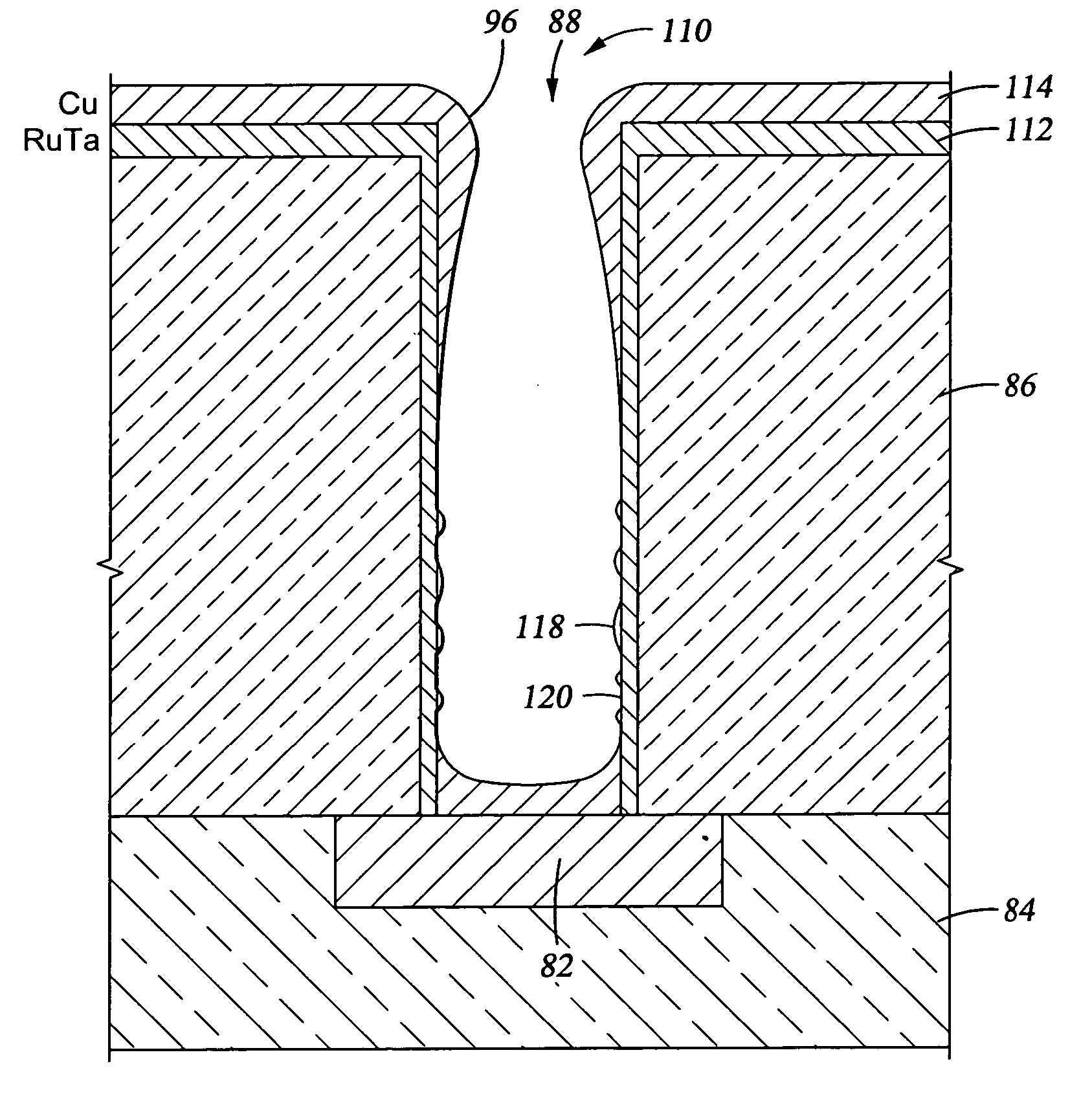
[0042] a novel copper interconnect liner structure 110 is illustrated in the cross-sectional view of FIG. 3. A barrier layer 112 of an alloy of ruthenium and tantalum is deposited directly over the upper-level dielectric layer 86 and onto the sidewalls of the via hole 88. The RuTa alloy is one type of a larger class of refractory noble alloys to be discussed later. A refractory noble alloy is a metal so it is electrically conductive and can be deposited by magnetron sputtering using a target of the desired alloy composition. A copper seed layer 114 is deposited over the RuTa barrier layer 112 to serve as a plating electrode and as a seed for the copper filled into the remaining portion of the via hole 88 by electrochemical plating (ECP). The excess copper deposited above the top of the via hole 88 is thereafter removed by chemical mechanical polishing (CMP). Although Sun et al. have suggested in U.S. Patent Application Publication 2006 / 0063375-A1 that a RuTa layer can serve as a see...

second embodiment

[0077] a contact liner structure 250, illustrated in the cross-sectional view of FIG. 14, includes the TaN barrier layer 182 in both the contact holes 224, 226 overlain by the compositionally differentiated near-noble refractory alloy layers 230, 236. Since the TaN barrier layer 182 may be commonly deposited into both contact holes 224, 226 by ALD, a joint 252 is required only between the two alloy layers 230, 236.

third embodiment

[0078] a contact liner structure 260, illustrated in the cross-sectional view of FIG. 15, eliminates the TaN barrier layer 182. Instead, two near-noble refractory alloy layers 230, 236 directly contact the dielectric layer 222 as well as the two wells 216, 218. This embodiment has the advantage of not needing the removal of the TaN barrier layer at the bottom of the two contact holes 224, 226.

[0079] The compositions are graded to better match the work functions of the p-contact layer 232 and the n-contact layer 238 to the p-well 216 and the n-well 218 respectively. Generally, a tantalum-rich RuTa alloy, that is, Ru−Ta+, has a work function better matched to n-type silicon and a ruthenium-rich RuTa alloy, that is, Ru+Ta−, has a work function better match to p-type silicon.

[0080] The RuTa layer, particularly when formed as an amorphous metal, allows the elimination of the copper seed layer. A copper metallization structure 270 illustrated in the cross-sectional view of FIG. 16 includ...


PUM

PropertyMeasurementUnit
pressureaaaaaaaaaa
thicknessaaaaaaaaaa
thicknessaaaaaaaaaa

Abstract

A fabrication method and a product for the deposition of a conductive barrier or other liner layer in a vertical electrical interconnect structure. One embodiment includes within a a hole through a dielectric layer a barrier layer of RuTaN, an adhesion layer of RuTa, and a copper seed layer forming a liner for electroplating of copper. The ruthenium content is preferably greater than 50 at % and more preferably at least 80 at % but less than 95 at %. The barrier and adhesion layers may both be sputter deposited. Other platinum-group elements substitute for the ruthenium and other refractory metals substitute for the tantalum. Aluminum alloying into RuTa when annealed presents a moisture barrier. Copper contacts include different alloying fractions of RuTa to shift the work function to the doping type.

Description

RELATED APPLICATION [0001] This application is a continuation in part of Ser. No. 11 / 124,611, filed May 5, 2005.FIELD OF THE INVENTION [0002] The invention relates generally to electrical interconnects including a barrier layer in semiconductor integrated circuits. In particular the invention relates to conductive metal barriers that are not subject to oxidation, such as amorphous metal barriers, or are conductive when oxidized and their sputter deposition. BACKGROUND ART [0003] Sputtering, alternatively called physical vapor deposition (PVD), is the most prevalent method of depositing layers of metals and related materials in the fabrication of silicon integrated circuits. One challenging application in the fabrication of advanced integrated circuits is the sputter deposition of thin liner layers in vertical electrical interconnects, usually called vias, for copper metallization. A conventional magnetron sputter reactor 10, illustrated schematically in cross section in FIG. 1, with...

Claims


Application Information

Patent Timeline
Patent Type & Authority Applications(United States)
IPC IPC(8): B32B7/00B32B3/00C23C16/00B05D5/12C23C14/00
CPCC23C14/046C23C14/0641Y10T428/24917Y10T428/24926C23C14/165H01L21/2855H01L23/53238H01L21/76844H01L21/76846H01L21/76873H01L2924/0002H01L23/485H01L21/76858H01L2924/00
Inventor WANG, RONGJUNCHUNG, HUATANG, XIANMINWANG, JENN YUEWANG, WEI D.TANAKA, YOICHIROYU, JICK M.GOPALRAJA, PRABURAM
Owner APPLIED MATERIALS INC
Why Eureka
Try Eureka