

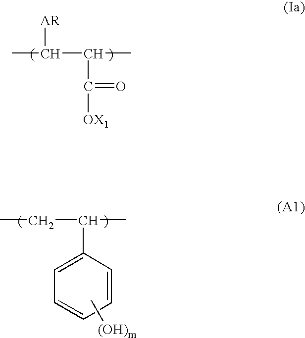
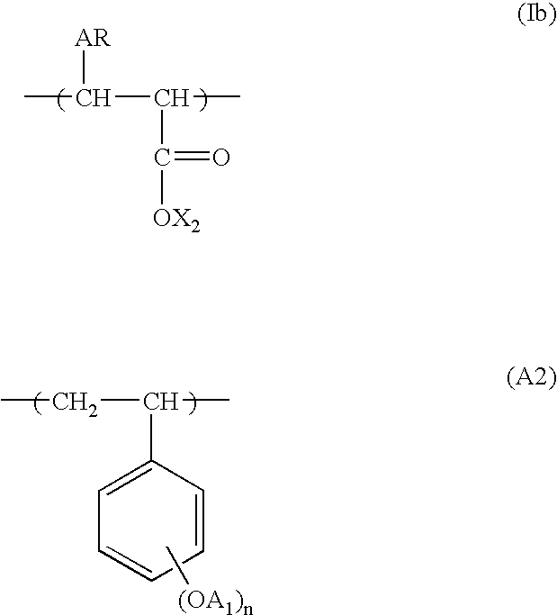
Positive resist composition and pattern forming method using the same
a technology of composition and resist, applied in the field of positive resist composition, can solve the problems of inability to meet all high sensitivity, high resolution, and disadvantageous narrowing of the process margin at the actual pattern formation, and achieve the effects of positive resist, high sensitivity, and enhanced performance at the fine processing of a semiconductor devi
- Summary
- Abstract
- Description
- Claims
- Application Information
AI Technical Summary
Benefits of technology
Problems solved by technology
Method used
Image


Examples
example 1
[0160]
(1) Preparation and Coating of Positive ResistResin A-2 0.93 gSulfonic Acid Generator B-20.065 gCarboxylic Acid Generator C-20.005 g
[0161] These components were dissolved in 8.8 g of propylene glycol monomethyl ether acetate, and 0.003 g of D-1 (see below) as the organic basic compound and 0.001 g of Megafac F176 (produced by Dainippon Ink & Chemicals, Inc., hereinafter simply referred to as “W-1”) as the surfactant were further added thereto and dissolved. The obtained solution was microfiltered through a membrane filter having a pore size of 0.1 pm to obtain a resist solution.
[0162] This resist solution was coated on a 6-inch silicon wafer by using a spin coater, Mark 8, manufactured by Tokyo Electron Ltd. and then baked at 110° C. for 90 seconds to obtain auniform film having a thickness of 0.25 μm.
(2) Production of Positive Resist Pattern
[0163] This resist film was then irradiated with electron beams by using an electron beam image-drawing apparatus (HL750, manufacture...
example 14
[0178] The preparation and coating of a resist shown in Table 3 were performed thoroughly in the same manner as in Example 1 to obtain a resist film. However, the film thickness was changed to 0.40 μm.
(3) Formation of Positive Pattern
[0179] The resist film obtained was pattern-exposed by using a KrF excimer laser stepper (FPA-3000EX-5, manufactured by Canon Inc., wavelength: 248 nm). The processing after the exposure was performed in the same manner as in Example 1. The evaluation of the pattern was performed as follows.
(3-1) Sensitivity
[0180] The cross-sectional profile of the pattern obtained was observed by using a scanning electron microscope (S-4300, manufactured by Hitachi, Ltd.). The minimum irradiation energy for resolving a 0.18-μm line (line:space=1:1) was defined as the sensitivity.
(3-2) Resolving Power
[0181] The limiting resolving power (the line and space were separated and resolved) at the irradiation dose of giving the above-described sensitivity was defined ...
PUM
| Property | Measurement | Unit |
|---|---|---|
| carbon number | aaaaa | aaaaa |
| molar ratio | aaaaa | aaaaa |
| molar ratio | aaaaa | aaaaa |
Abstract
Description
Claims
Application Information