Also, in order to improve
image quality, it is desirable to use larger pixel circuits, which further leads to an increase in the length of the memory.
A further difference between memory used in high speed
CMOS image sensor circuits and memory typically used in other applications is that the memory for high speed
CMOS image sensor circuits is usually configured to accept large amounts of data in parallel from a large number of column ADC circuits, while other types of memory are usually not designed to accept as much data in parallel.
The
high resistance of the bit lines due to the long lengths of the bit lines and the
high capacitance of the bit lines due to the large number of memory cells connected to the bit lines may lead to
signal degradation, and may impose
physical limitations on a speed of memory readout operations.
Moreover, when bit lines of a readout
bus from memory are extremely long and, for example, span the length of a pixel array, an additional problem is created in that data signals must travel across the length of the bit lines to sense amplifiers, and then are driven by pad drivers to pads that may be located in various positions all over the image sensor circuit.
Such a situation is especially problematic when signals must be driven by pad drivers to pads that are located in locations, with respect to the sense amplifiers, that are in the opposite direction of the direction in which the data signals travel across the bit lines from the memory cells to the sense amplifiers.
Driving the data signals over longer distances may result in
higher power consumption to drive the signals, and may also lead to the injection of
noise into a substrate that is part of the image sensor circuit.
Such
skew time may not be a very severe issue when a
system clock is less than 100 MHz, but such
skew time will become a severe issue as
system clocks for image sensor circuits are increased to 200 MHz and higher.
However, in high speed
CMOS image sensor circuit designs, even with the number of memory cells connected to a readout bus reduced in half, the number of memory cells connected to the readout bus may still be on the order of, for example, 500 to 1,000 memory cells, which may still result in a large amount of
capacitance.
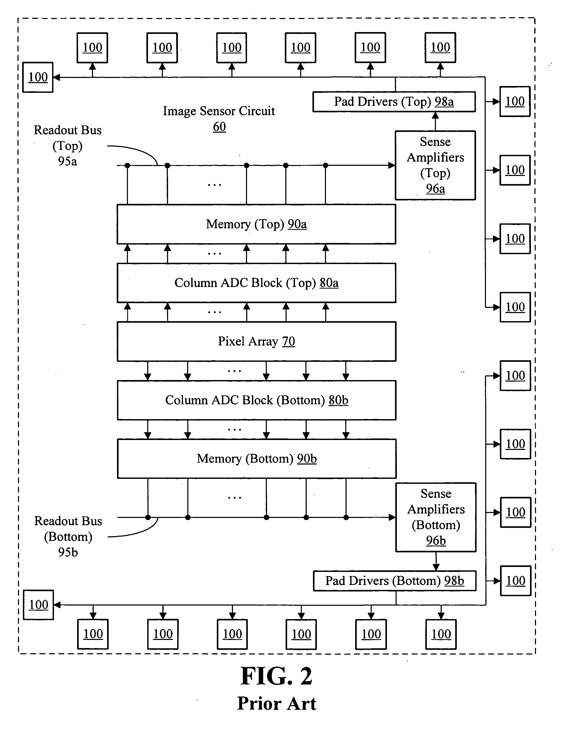
Furthermore, even in configurations with both the top memory 90a and the bottom memory 90b, there is still the problem that the top readout bus 95a and the bottom readout bus 95b span the length of the pixel array 70.
The driving of signals across the image sensor circuit 60 results in high
power consumption, and may result in the injection of digital
noise into a substrate that is part of the image sensor circuit 60.
Thus, such a configuration still has the problems that are associated with long readout buses as discussed above.
While memory readout operations are one
bottleneck that limits the increasing of imager speed, another
bottleneck is the amount of time needed to send control signals from an ADC controller to all column ADC circuits in a column ADC block.
The time needed for control signals to reach all column ADC circuits from an ADC controller further imposes a limit on an increasing of imager speed.
However, there has been a problem with paneling in CCD technology in that a discontinuity between panels of pixels may result in an image non-uniformity at the boundaries of the panels.
Such image non-uniformities may be unacceptable to end users.
Also, a difference between the amplifiers serving separate panels and a difference in local parasitic effects between panels may result in response non-uniformities between the panels.
The problems arise due in part to the splitting of pixel arrays into separate panels, where each pixel array outputs analog signals.
