Stripping and cleaning of organic-containing materials from electronic device substrate surfaces

a technology of electronic devices and substrate surfaces, which is applied in the direction of cleaning using liquids, inorganic non-surface active detergent compositions, instruments, etc., can solve the problems of unacceptably slow removal rate of organic materials and high corrosion rate of metals present on the substrate surface, and achieve the effect of reducing the odor of solvents

Inactive Publication Date: 2007-05-03
APPLIED MATERIALS INC
View PDF20 Cites 11 Cited by
  • Summary
  • Abstract
  • Description
  • Claims
  • Application Information

AI Technical Summary

Benefits of technology

[0041] Like ethylene carbonate, propylene carbonate is odorless and colorless. However, propylene carbonate is a liquid at room temperature. The disadvantage of propylene carbonate is that it is less soluble in the propionic acid solutions discussed above. The addition of ethylene carbonate or propylene carbonate to a propionic acid-comprising solvent tends to further reduce the odor of the solvent, providing an advantage when a vented but open stripping process is used.

Problems solved by technology

If the stripping solution contains too little ozone, the organic material removal rate will be unacceptably slow.
If the stripping solution contains too much ozone, the corrosion rate of metals present on the substrate surface may be too high.

Method used


Image

  • Stripping and cleaning of organic-containing materials from electronic device substrate surfaces
  • Stripping and cleaning of organic-containing materials from electronic device substrate surfaces
  • Stripping and cleaning of organic-containing materials from electronic device substrate surfaces

Examples


example one

Removal of Photoresist from a Substrate Surface Using Ozonated Pure Propionic Acid

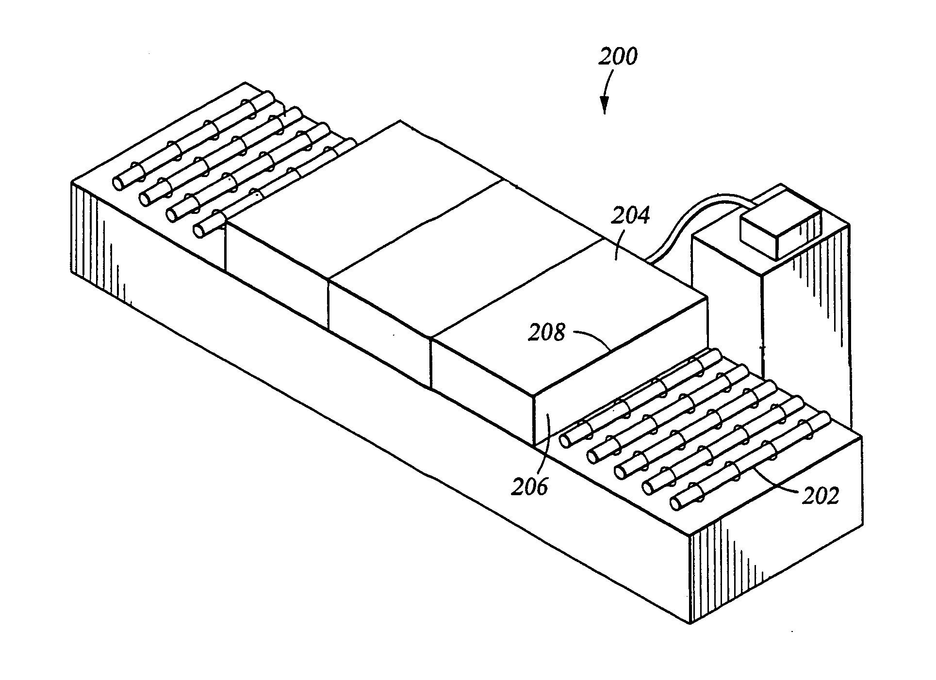
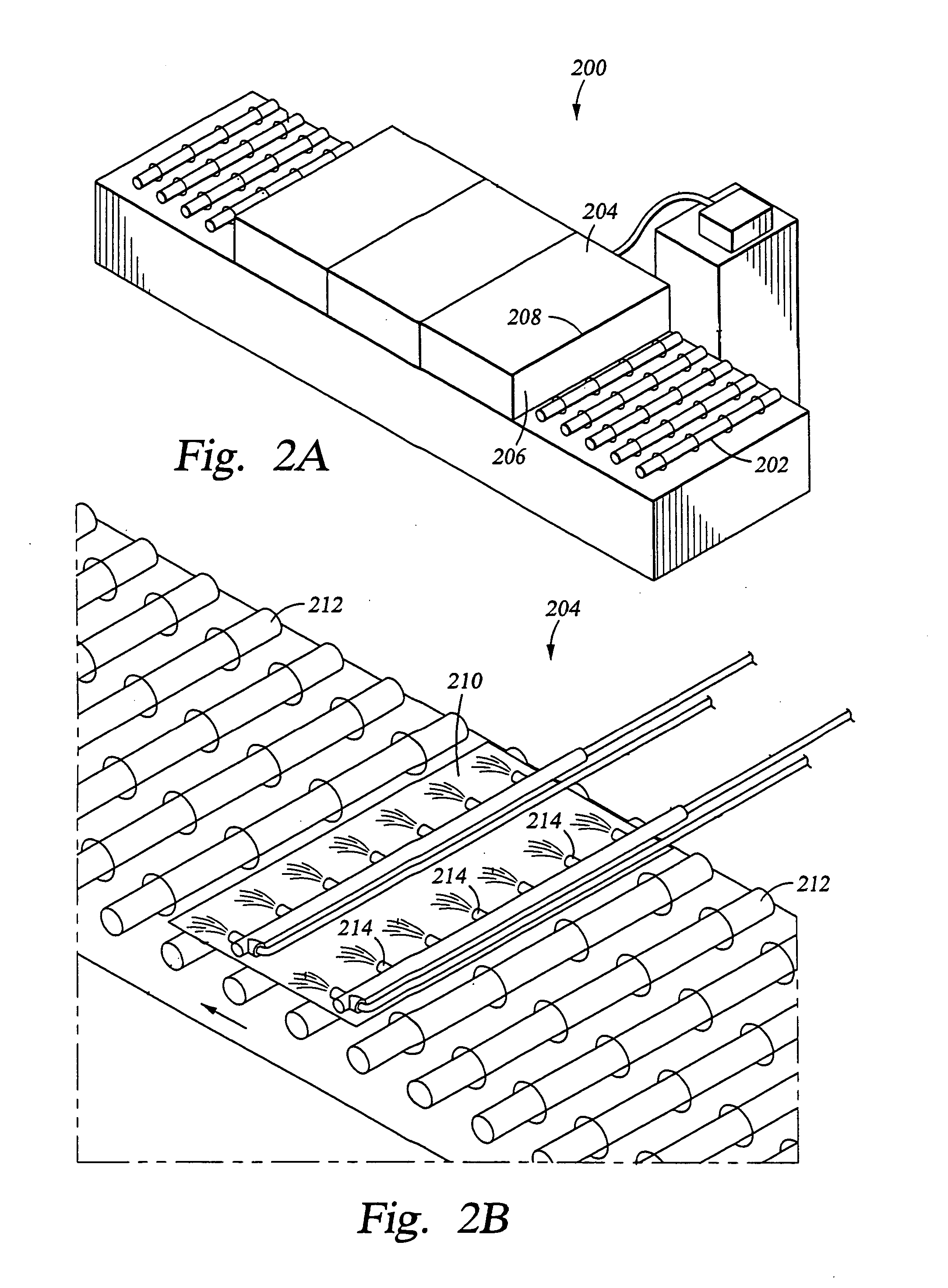
[0075] A layer of a deep ultra-violet (DUV) photoresist which is sensitive to 248 nm radiation (UV 6, available from Shipley, Marlborough, MA) was applied to a thickness of approximately 10,000 Å onto the surface of a single-crystal silicon wafer. The photoresist was applied using a spin-on process, then baked for 30 minutes at 95° C. Ozonated propionic acid (100% propionic acid) containing at least 300 ppm (or mg / L) of ozone was sprayed onto the surface of the photoresist-coated substrate at room temperature (25° C.), using a dispensing system such as that shown in FIG. 2B. The ozonated propionic acid was allowed to react with the photoresist for a period of 30, 60, or 120 seconds, then rinsed off the substrate surface by spraying with deionized water for a period of 10 to 20 seconds.

[0076] Table Three, below, shows the amount of photoresist which was removed from each substrate. Within the accuracy...

example two

Corrosivity of Ozonated Propionic Acid on Aluminum

[0078] A layer of aluminum was deposited to a thickness of approximately 10,000 Å onto the surface of a single-crystal silicon wafer using a physical vapor deposition (PVD) process of the kind known in the art. To test the corrosivity of ozonated propionic acid on aluminum, ozonated propionic acid (100% propionic acid) containing at least 300 ppm (or mg / L) of ozone was sprayed onto the surface of the aluminum-coated substrate at room temperature (25° C.), using a dispensing system such as that shown in FIG. 2B. The ozonated propionic acid was allowed to react with the aluminum for a period of 30, 60, or 120 seconds, then rinsed off the substrate surface by spraying with deionized water for a period of 10 to 20 seconds.

[0079] Table Four, below, shows the thickness of the aluminum layer before and after treatment.

TABLE FOURCorrosivity of Ozonated Propionic Acid Stripping Solutionon AluminumPre-TreatmentPost-TreatmentAl ThicknessTre...

example three

Corrosivity of Ozonated Propionic Acid on Titanium Nitride

[0081] A layer of titanium nitride was deposited to a thickness of 450 Å onto the surface of a single-crystal silicon wafer using a physical vapor deposition (PVD) process. In order to test the corrosivity of ozonated propionic acid on titanium nitride, ozonated propionic acid (100% propionic acid) containing at least 300 ppm (or mg / L) of ozone was sprayed onto the surface of the TiN-coated substrate at room temperature (25° C.), using a dispensing system such as that shown in FIG. 2B. The ozonated propionic acid was allowed to react with the titanium nitride surface for a period of 30, 60, or 120 seconds, then rinsed off the substrate surface by spraying with deionized water for a period of 10 to 20 seconds.

[0082] Table Five, below, shows the thickness of the titanium nitride layer before and after treatment.

TABLE FIVECorrosivity of Ozonated Propionic Acid Cleaning Solutionon Titanium NitridePre-TreatmentPost-TreatmentTi...


PUM

PropertyMeasurementUnit
volume %aaaaaaaaaa
vapor pressureaaaaaaaaaa
temperatureaaaaaaaaaa

Abstract

Disclosed herein is a method of removing an organic material from an electronic device substrate surface. The method is particularly useful when the device substrate includes exposed metal. According to the present method, an electronic device substrate surface is exposed to a solution comprising ozone (O3) at a concentration ranging from about 45 ppm to about 600 ppm in a solvent consisting of pure propionic acid or propionic acid in combination with deionized water or a carbonate having from 2 to 4 carbons. The method is particularly useful in the manufacture of large surface areas covered with device structures, such as electronic TFT flat panel displays, solar cell arrays, and structures containing light-emitting diodes. The method is also useful for removing organic materials from the surface of solid state device-containing semiconductor substrates.

Description

BACKGROUND OF THE INVENTION [0001] 1. Field of the Invention [0002] The invention relates to a method of removing organic-containing materials such as photoresists, high temperature organic layers, and organic dielectric materials from an electronic device substrate surface. The method is particularly useful in the manufacture of large surface areas covered with device structures, such as electronic TFT flat panel displays, solar cell arrays, structures containing light-emitting diodes, and semiconductor wafers. [0003] 2. Brief Description of the Background Art [0004] The fabrication of electronic device structures is complicated by the number of different materials which are used, both to provide the elements of the functional device, and as temporary process structures during fabrication of the device. Since most of the devices involve the formation of layers of inter-related, intricate, patterned structures, photoresists and high temperature organic masking materials are commonly...

Claims


Application Information

Patent Timeline
Patent Type & Authority Applications(United States)
IPC IPC(8): B08B3/00C23G1/00C23D17/00
CPCC11D3/3942C11D7/02C11D7/265C11D7/5022C11D11/0047G03F7/423H01L21/31133H01L21/31138H01L31/18
Inventor VERHAVERBEKE, STEVEN
Owner APPLIED MATERIALS INC
Why Eureka
Try Eureka