

Method and apparatus for producing large, single-crystals of aluminum nitride
- Summary
- Abstract
- Description
- Claims
- Application Information
AI Technical Summary
Benefits of technology
Problems solved by technology
Method used
Image

Examples
example — 260
Example—260 nm Laser Diode Fabrication
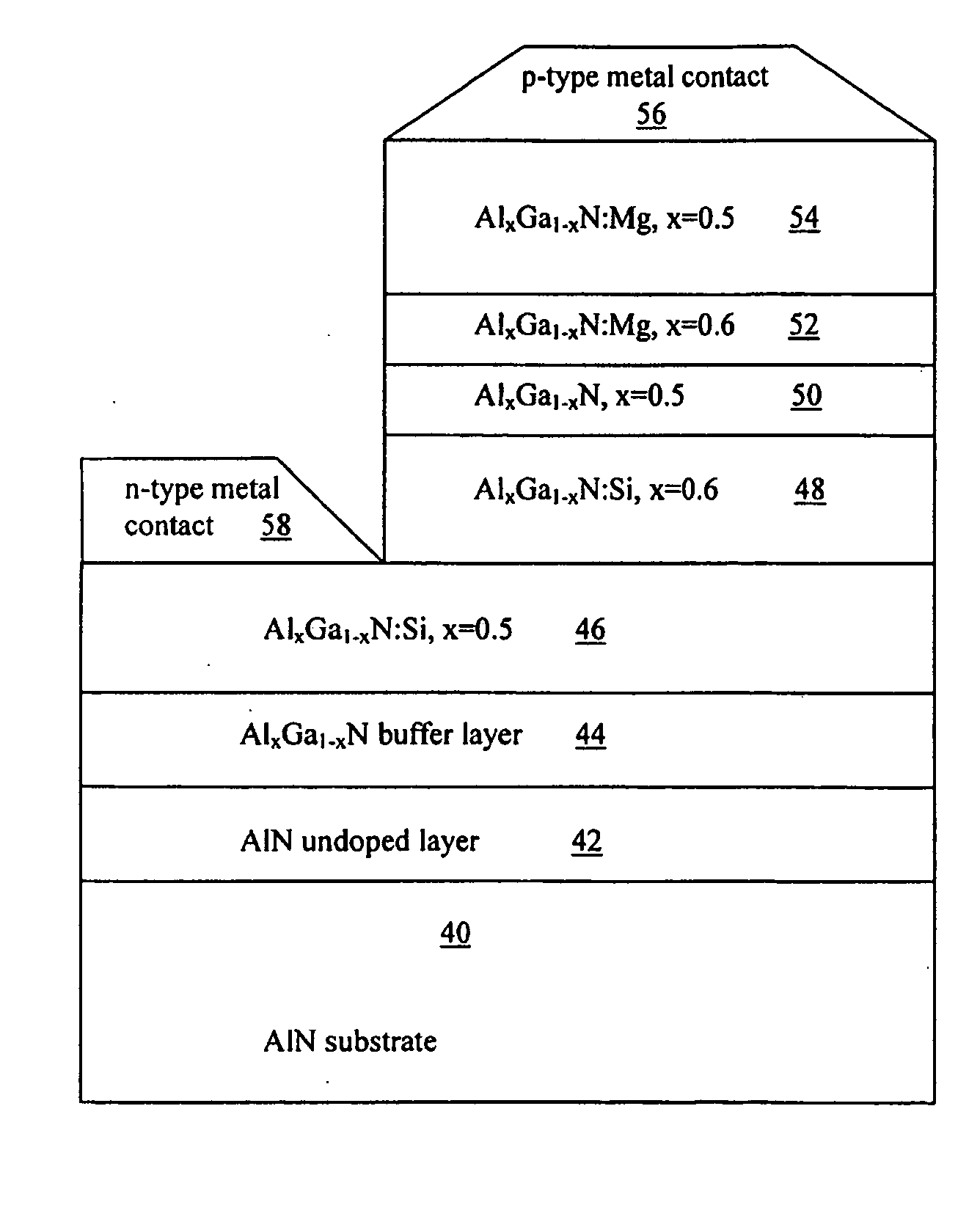
[0089]FIG. 6 is a schematic cross-sectional view of a portion of a 260-nm laser diode fabricated using the method of the present invention. Initially, low defect density AlN substrate 40, which is prepared using the method discussed above, is polished by CMP. The polished substrate is then introduced into a conventional OMVPE system. The surface of the low defect density AlN substrate is cleaned to remove any oxide or other impurities on the crystal surface by heating the substrate at a temperature of 1150° C. for 20 min under ammonia plus nitrogen or hydrogen plus nitrogen flow prior to growth. An epitaxial layer 42 of AlN having a thickness of about 100 nm is then grown on the substrate to improve its surface quality before starting to grow the device layers. Next, an undoped AlxGa1-xN buffer layer 44 having a thickness of approximately 1 μm is grown atop the epitaxial AlN layer to relieve lattice mismatch through the formation of misfit dislo...
PUM
 Abstract
Description
Claims
Application Information