High-temperature solder, high-temperature solder paste and power semiconductor device using same

a technology of high-temperature solder and semiconductor devices, which is applied in the direction of soldering apparatus, semiconductor/solid-state device details, manufacturing tools, etc., can solve the problems of difficult to directly apply high-temperature solder to the assembly of semiconductor devices, and achieve excellent wettability, easy supply, and excellent temperature cycle

Inactive Publication Date: 2007-06-07
HITACHI LTD
View PDF4 Cites 46 Cited by
  • Summary
  • Abstract
  • Description
  • Claims
  • Application Information

AI Technical Summary

Benefits of technology

[0010] The present invention intends to provide the solder excellent in wettability with respect to Ni and Cu, the wettability being a property required for the high-temperature solder, the solder satisfying junction temperature ≦400° C., preferably junction temperature ≦370° C., heat resistant temperature ≧280° C., and moreover the solder being excellent in the temperature cycle life and high-temperature reliability with respect to Cu or Ni.
[0011] The present invention intends to provide the solder paste material, which can be easily supplied to the junction part without damaging the wettability with respect to Ni or Cu under inert atmosphere or reduction atmosphere and at the bonding conditions in the range of 350° C. to 400° C., and which can eliminate residual liquid remaining at the junction part after bonding as much as possible.
[0012] The present invention intends to provide power semiconductor devices without using lead, which have the reflow resistance at 260° C., the heat resistant reliability under the conditions of 200° C. and 1000 hr or more, and high reliability for the high-temperature cycle.

Problems solved by technology

If these properties are not provided, it is difficult to directly apply the high-temperature solder to the assembly of the semiconductor devices.

Method used


Image

  • High-temperature solder, high-temperature solder paste and power semiconductor device using same
  • High-temperature solder, high-temperature solder paste and power semiconductor device using same
  • High-temperature solder, high-temperature solder paste and power semiconductor device using same

Examples


example 1

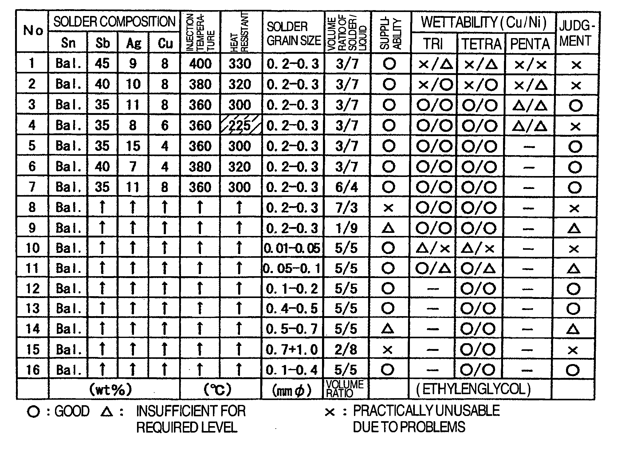
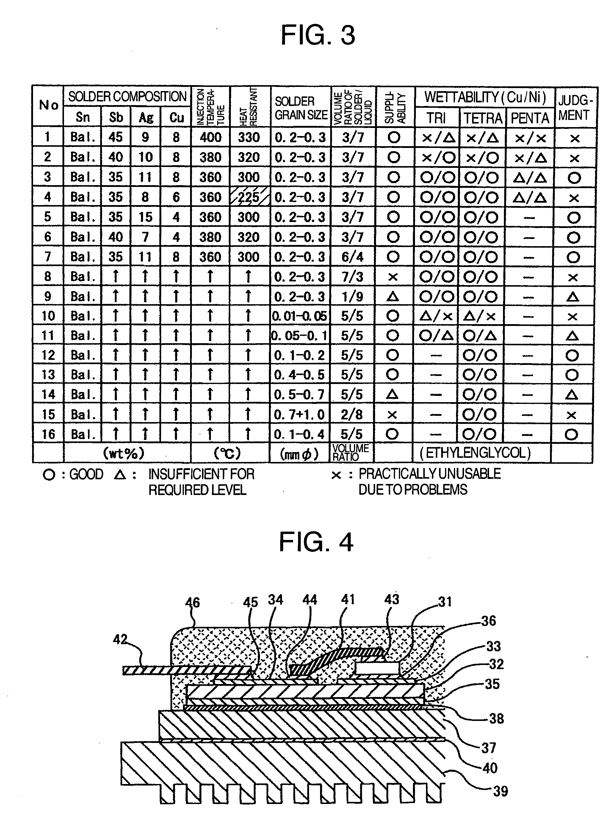
[0039] The high-temperature solder material of this example which was composed of Sn, Sb, Ag, and Cu as the main constitutive elements and the rest of other unavoidable impurity elements has the composition defined in the range of 42 wt %≦Sb / (Sn+Sb)≦48 wt %, 5 wt %≦Ag<20 wt %, 3 wt %≦Cu<10 wt %, and Ag+Cu≦25 wt %. Moreover, at least one element selected from the group consisting of Ni, Ge, and Ga of 0.01 wt % to 5.0 wt % and P of 0.005 wt % to 0.5 wt % were added to the high-temperature solder material with the above-described composition.

[0040] As a result of manufacturing a variety of alloys of the above-described composition by way of trial and investigating the solidus and liquidus temperatures, it was found that the solidus temperature is determined by the composition ratio of Sn and Sb, and is 280° C. or more within the above-described composition range, that a further addition of Ag or Cu hardly decreases the solidus temperature but can reduce only the liquidus temperature, ...

example 2

[0051] In this example, in order to provide a solder paste material which can be easily supplied to the junction part without damaging the wettability to Ni or Cu under the conditions of inert atmosphere or reduction atmosphere and at junction temperature in the range of 350° C. to 400° C. and which can eliminate residual liquid remaining at the junction part after the bonding as much as possible, the high-temperature solder paste material which an organic material of a liquid or cream form was mixed was provided, wherein the high-temperature solder paste material was composed of the high-temperature solder of Example 1 and any one or more kinds of materials selected from an ethylene glycol group, an alcoholic group, and a glycerol group whose molecules are constituted from atoms of only C, O, H. Moreover, the grain size (granularity) of the high-temperature solder was set to the range of 0.05 mmφ to 0.5 mmφ, preferably to the range of 0.1 mmφ to 0.5 mmφ, and an organic material who...

example 3

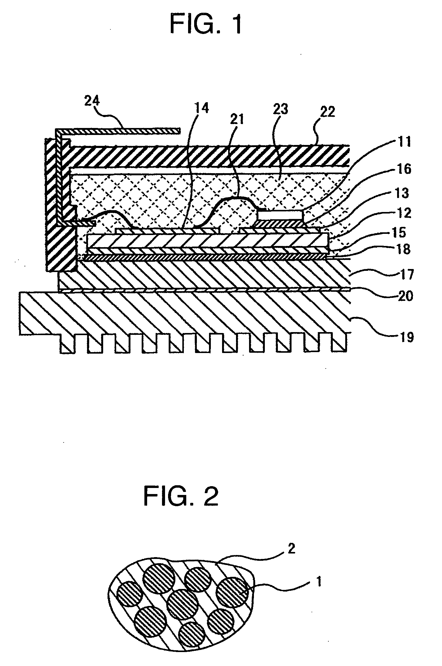
[0061]FIG. 1 shows an example of the sectional structure of a power semiconductor module according to this example. In FIG. 1, a power semiconductor device 11, such as an IGBT, a diode, and a power MOSFET formed in a Si semiconductor chip is mounted on a ceramic substrate 12, and furthermore is mounted on a heat sink 17. The power semiconductor device 11 and the ceramic substrate 12 are bonded by an Sn—Sb—Ag—Cu system high-temperature solder 16 according to Example 1 via a metallic circuit pattern 13. The ceramic substrate 12 and the heat sink 17 are bonded by a moderate temperature solder 18 made of Sn—Ag—Cu (melting-point in the range of 217° C. to 222° C.) via a metal solid pattern 15. The main-current electrode and control electrode of the power semiconductor device are connected to another metallic circuit pattern 14 on the ceramic substrate 12 by an Al wire 21.

[0062] To the heat sink 17 is attached a resin case 22, which is integrally molded with an external lead 24, and a ge...


PUM

PropertyMeasurementUnit
boiling pointaaaaaaaaaa
grain diameteraaaaaaaaaa
melting pointaaaaaaaaaa

Abstract

The present invention intends to provide a power semiconductor device using a high-temperature lead-free solder material, the high-temperature lead-free solder material having the heat resistant property at 280° C. or more, and the bondability at 400° C. or less, and excellent in the suppliabilty and wettability of solder, and in the high-temperature storage reliability and the temperature cycle reliability. In the power semiconductor device according to the present invention, a semiconductor element and a metal electrode member were bonded each other by a high-temperature solder material comprising Sn, Sb, Ag, and Cu as the main constitutive elements and the rest of other unavoidable impurity elements wherein the high-temperature solder material comprises 42 wt %≦Sb/(Sn+Sb)≦48 wt %, 5 wt %≦Ag<20 wt %, 3 wt %≦Cu<10 wt %, and Ag+Cu≦25 wt %.

Description

FIELD OF THE INVENTION [0001] The present invention relates to a lead-free solder material for which a high melting point of 280° C. or more is required, and to power semiconductor devices using the lead-free solder material. BACKGROUND OF THE INVENTION [0002] Conventionally, a high melting-point lead solder which contains lead of 90% or more and other Sn, Ag, etc. of several % and exhibits the melting-point of 280° C. or more has been used at the junction between a power semiconductor device and an external electrode. In recent years, it has become important to protect environment from contamination of harmful substances, and thus the removal of lead from the assembly members of electronic devices is required. However, a high-temperature solder without using lead, the high-temperature solder capable of directly replacing a lead-contained high-temperature solder, has not yet been developed. In the circumstances high-temperature solders of a Zn—Al system, Sn—Sb system, and Bi—Ag syst...

Claims


Application Information

Patent Timeline
Patent Type & Authority Applications(United States)
IPC IPC(8): C22C13/02
CPCB23K35/025B23K35/262B23K35/3006B23K35/302C22C13/02H01L23/49513H01L24/01H01L24/29H01L24/32H01L24/33H01L24/40H01L24/45H01L24/48H01L24/81H01L24/83H01L24/84H01L2224/05111H01L2224/05639H01L2224/05647H01L2224/13147H01L2224/16225H01L2224/29298H01L2224/32225H01L2224/32245H01L2224/45124H01L2224/48091H01L2224/48227H01L2224/48247H01L2224/48472H01L2224/4911H01L2224/73265H01L2224/81065H01L2224/81075H01L2224/81097H01L2224/81805H01L2224/83065H01L2224/83075H01L2224/83097H01L2224/83203H01L2224/83211H01L2224/83801H01L2924/01004H01L2924/01005H01L2924/01006H01L2924/01007H01L2924/01009H01L2924/01013H01L2924/01014H01L2924/01015H01L2924/01022H01L2924/01027H01L2924/01028H01L2924/01029H01L2924/0103H01L2924/01031H01L2924/01032H01L2924/01033H01L2924/01047H01L2924/0105H01L2924/01051H01L2924/01073H01L2924/01078H01L2924/01079H01L2924/01082H01L2924/01083H01L2924/01322H01L2924/014H01L2924/13055H01L2924/13091H01L2924/19041H01L2924/19105H01L2924/19107H01L2924/20108H01L2924/30105H01L2924/0132H01L24/49H01L2224/2919H01L2224/83455H01L2924/00013H01L2924/01023H01L2924/01024H01L2924/0665H01L2224/29101H01L2924/0134H01L2224/29111H01L2924/0133H01L2224/83447H01L2924/15787H01L2224/48739H01L2224/48747B23K35/02B23K35/22H01L2224/0401Y10T428/12528Y10T428/12708H01L2924/00014H01L2224/13099H01L2924/00H01L2924/00012H01L2924/01026H01L2924/3512H01L2224/29099H01L2224/29199H01L2224/29299H01L2224/2929H01L2924/351H01L2224/29294H01L2924/181H01L2224/40225H01L24/73H01L2224/40091H01L2224/37599H01L2224/371H01L2224/84801H01L2224/37147H01L2224/376H01L24/37H01L2224/2612H01L2224/73221
Inventor KAJIWARA, RYOICHIITOU, KAZUTOSHI
Owner HITACHI LTD
Why Eureka
Try Eureka