

Annealed wafer and manufacturing method of annealed wafer
a technology of annealing wafers and manufacturing methods, which is applied in the direction of crystal growth process, after-treatment details, and under a protective fluid, etc., can solve the problems of less device yield, less device yield, and inferior annealing wafers
- Summary
- Abstract
- Description
- Claims
- Application Information
AI Technical Summary
Benefits of technology
Problems solved by technology
Method used
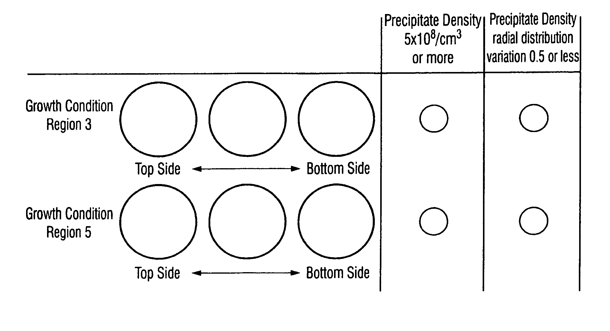
Image

Examples
example
[0089] Silicon single crystal manufacturing apparatuses used in this example are those used in general silicon single crystal manufacturing according to the CZ method. The apparatuses are a first pulling furnace in which a heat shielding plate is cooled in a particular method in order to increase the cooling speed of 1100 to 1000° C. and a second furnace having a general cooling speed. When the present disclosure is to be carried out, no particular limitations are imposed on the pulling furnaces as long as the growth conditions of the present disclosure can be carried out.
[0090] A silicon single crystal grown by utilizing the apparatuses has a conduction type: p-type (boron doped) and a crystal diameter: 8 inches (200 mm).
[0091] Nitrogen doping was performed by putting substrates having nitride films in silicon melts.
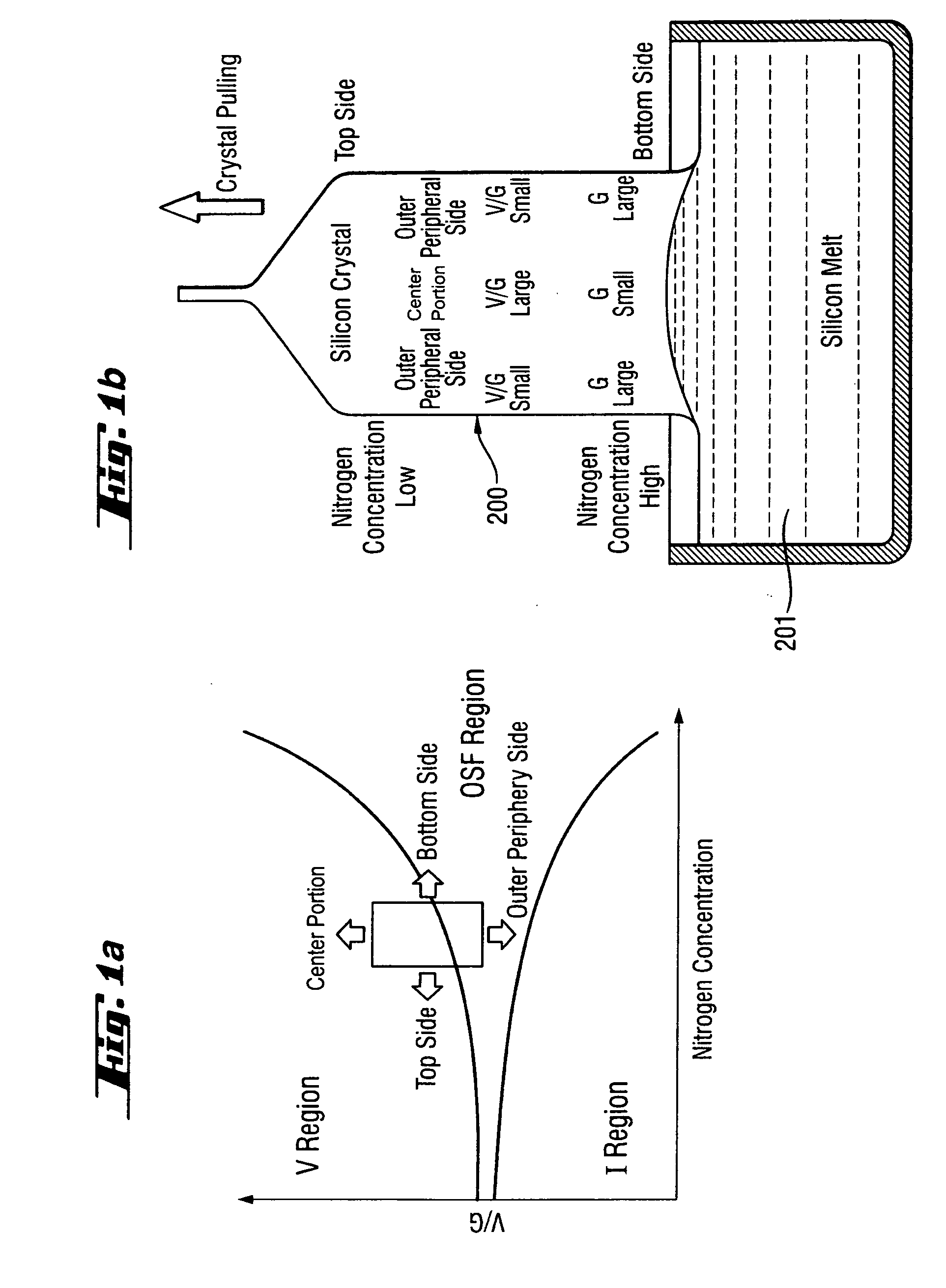
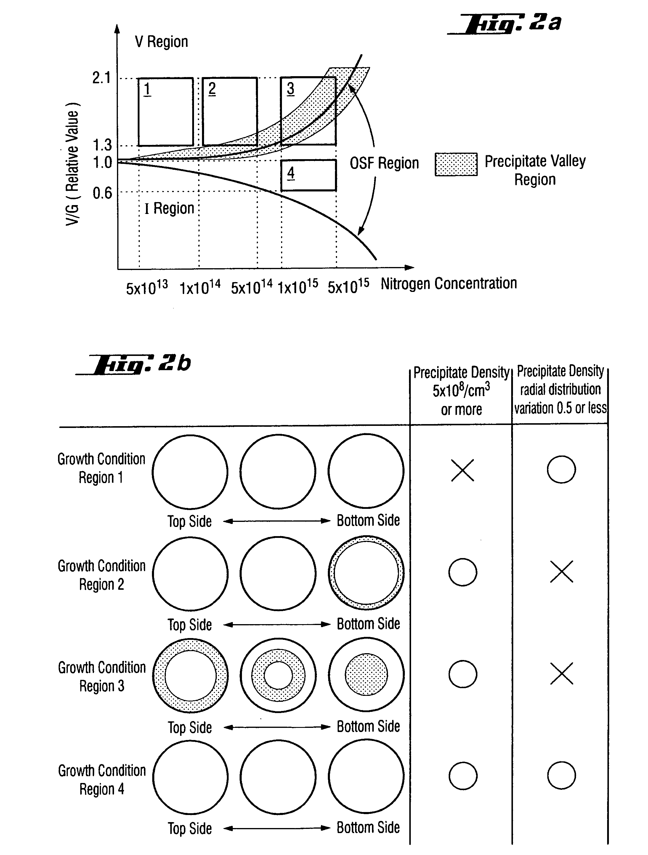
[0092] Relative V / G values are defined in the following manner. In a pulling furnace having the same structure as the furnace in which the nitrogen doped crystal was...
PUM
 Abstract
Description
Claims
Application Information