Control signal interface circuit for computer memory modules

a control signal and memory module technology, applied in the field of computer memory modules, can solve the problems of effectively limiting memory access speeds, affecting the performance of memory access speeds, and requiring increased latency, so as to achieve easy realization, wide band operation, and small gain variation

Inactive Publication Date: 2007-08-09
WASHBURN ROBERT D +1
View PDF11 Cites 0 Cited by
  • Summary
  • Abstract
  • Description
  • Claims
  • Application Information

AI Technical Summary

Benefits of technology

[0012] One embodiment contains a variety of circuit topologies more typically associated with linear, analog, amplifier circuits than digital logic. These include differential amplifiers, cascode structures, level shifting, complimentary emitter follower output drive, and feedback. As a result, a linear, low distortion, wideband video amplifier embodiment can be easily realized by adjustment of bias and device DC operating points, value changes, and changes to the means by which ancillary circuit functions are implemented. The result is a video amplifier capable of very wide band operation with little gain variation and very low distortion. The input impedance is both higher and flatter than achieved with typical operational amplifiers. The output looks substantially like a voltage source and is capable of stably driving capacitive loads of tens of picofarads with minimal signal distortion.

Problems solved by technology

The total capacitance has made it extremely difficult to achieve fast memory speeds.
In fact, the control-signal rise and fall times are typically greater than the entire clock period, forcing increased latency and effectively limiting memory access speeds.

Method used


Image

  • Control signal interface circuit for computer memory modules
  • Control signal interface circuit for computer memory modules
  • Control signal interface circuit for computer memory modules

Examples


Embodiment Construction

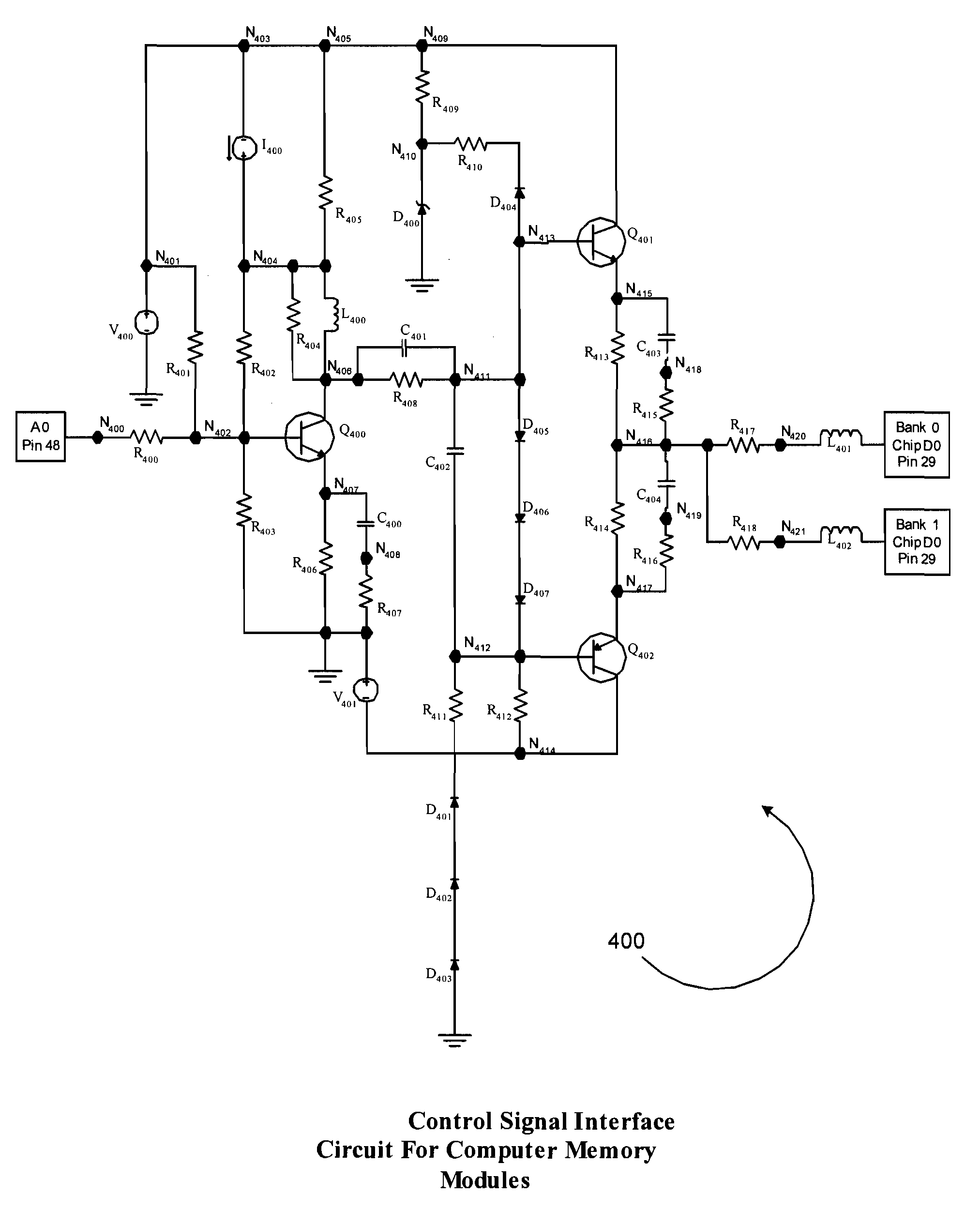
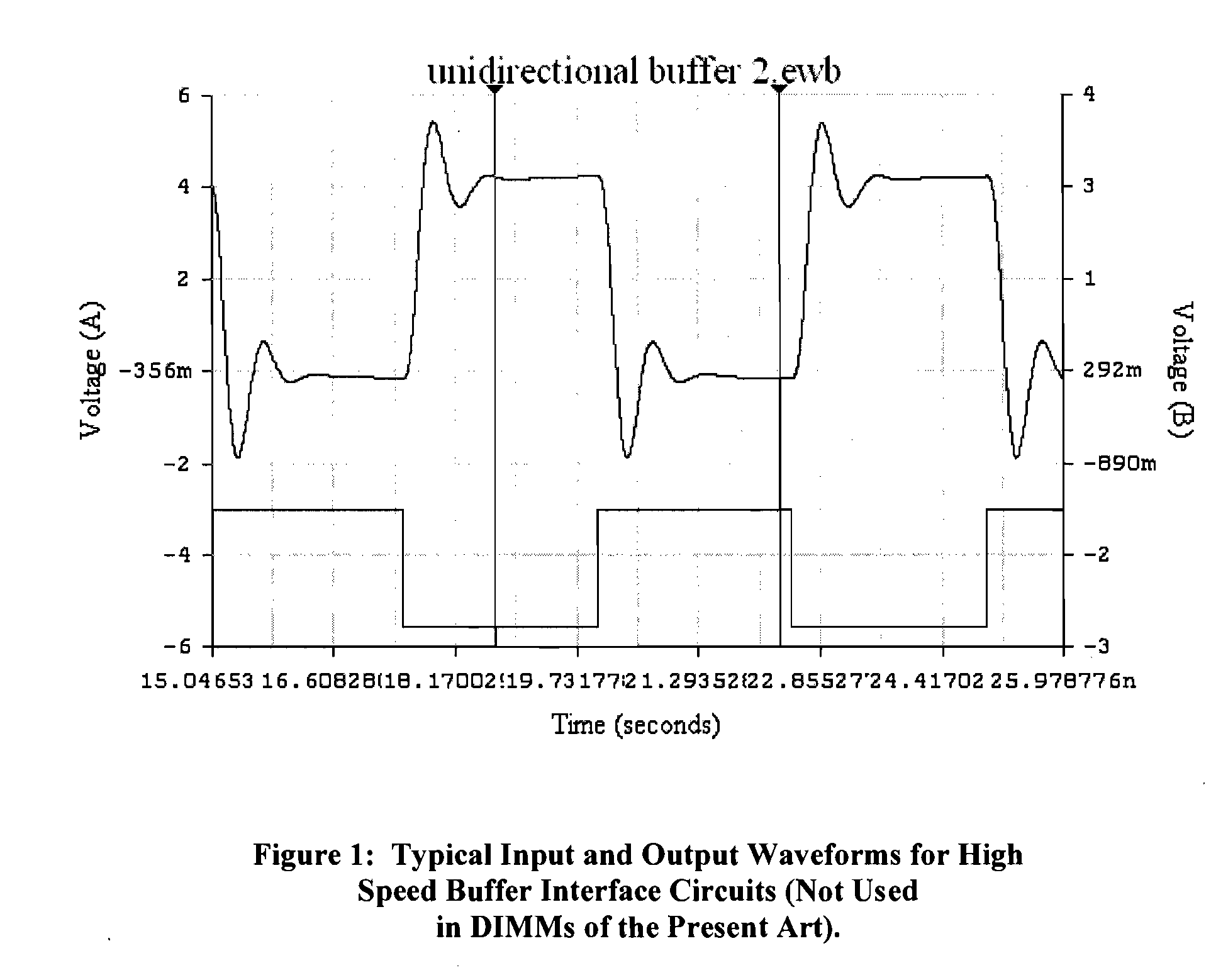
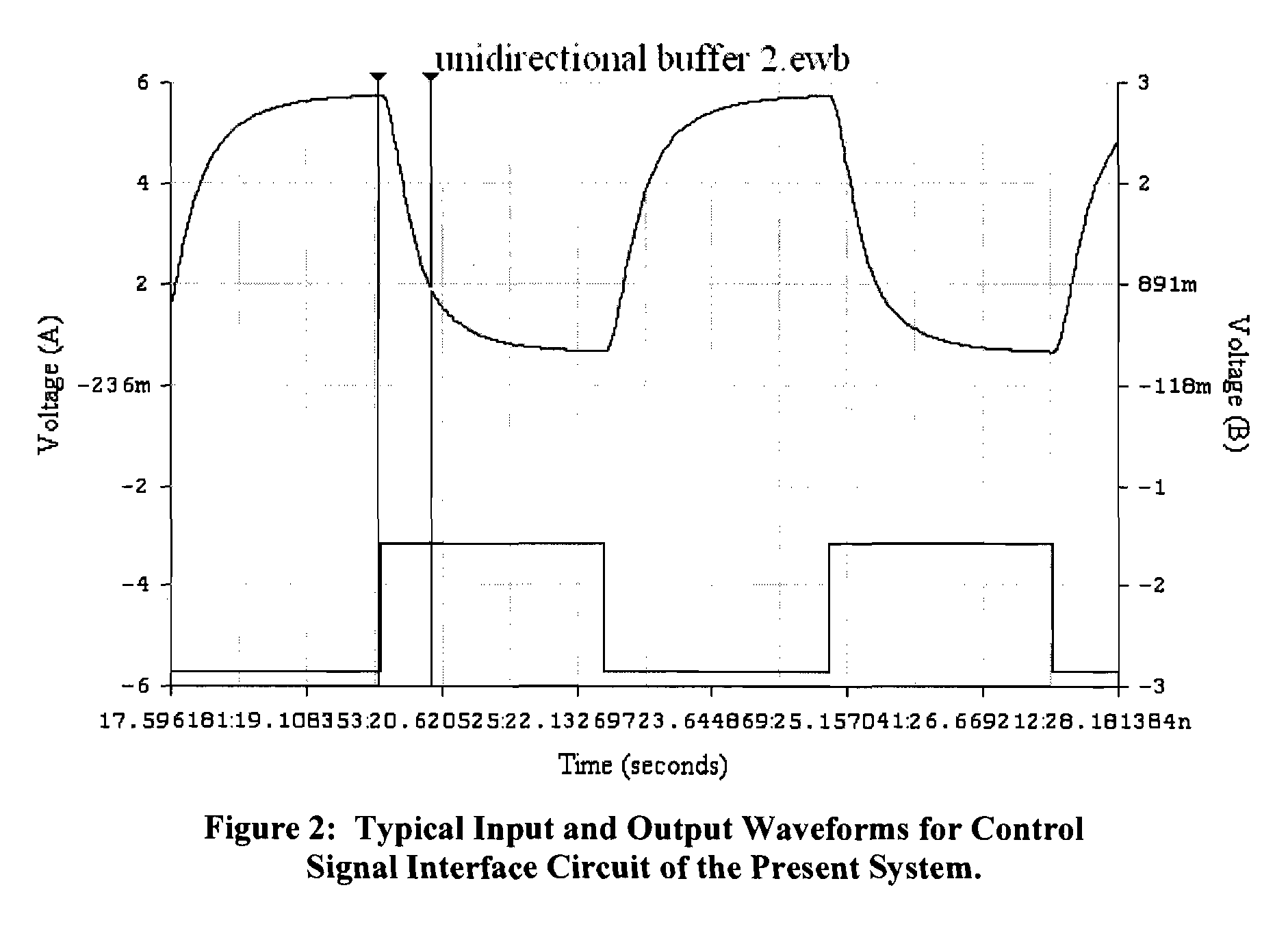
[0024] The present system is a high speed, low input capacitance interface circuit. It is directed toward coupling unidirectional control signals from the input connector of a memory module to the appropriate pins of the memory devices on the module. In the following description, numerous specific details are set forth to provide a more thorough description of embodiments of the system. It is apparent, however, to one skilled in the art, that the system may be practiced without these specific details. In other instances, well known features have not been described in detail so as not to obscure the system.

[0025] Discussion of the present system is directed toward application to 184-pin, 2.5 Volt (VDD) / 2.5 Volt (VDDQ), Unbuffered, Non-ECC, Double Data Rate, Synchronous DRAM Dual In-Line Memory Modules (DDR SDRAM DIMMs), henceforth referred to as DIMMs. DIMMs are intended for use as main memory when installed in PCs and network servers. While the present discussion is directed toward...


PUM


Abstract

The present system is an electronic circuit designed for incorporation on high-speed computer memory modules such as DDR DIMMs. It couples control signals such as address bits, bank selects, enable and even clock signals between the module input connector and the memory devices. The circuit provides low propagation delay, fast rise and fall times with no overshoot or undershoot, and significantly improves timing control compared to memory modules of the present art. Capacitive loading on the motherboard is typically much less than that provided by a single memory device input and is independent of the number of memory devices per bank or the number of banks of memory devices on the memory module. For multiple memory modules connected to the memory bus, capacitive loading is essentially N times the equivalent loading for a single memory module.

Description

CROSS-REFERENCE TO RELATED APPLICATIONS [0001] This application claims the benefit of U.S. provisional patent application No. 60 / 730,947, filed Oct. 27, 2005, which is herein incorporated by reference in its entirety.COPYRIGHT NOTICE [0002] A portion of the disclosure of this patent document contains material that is subject to copyright protection. The copyright owner has no objection to the facsimile reproduction by anyone of the patent document or the patent disclosure, as it appears in the Patent and Trademark Office patent files or records, but otherwise reserves all copyright rights whatsoever. BACKGROUND OF THE SYSTEM [0003] 1. Field [0004] The system relates to the field of computer memory modules and to wideband, high frequency amplifiers. [0005] 2. Background Art [0006] Since the development of the personal computer, the characteristics and performance of the main memory has played a major role in defining the capabilities of the computers. From the beginning, the trend in...

Claims


Application Information

Patent Timeline
Patent Type & Authority Applications(United States)
IPC IPC(8): G11C29/00
CPCG11C5/04G11C7/1066G11C5/063
Inventor WASHBURN, ROBERT D.MCCLANAHAN, ROBERT F.
Owner WASHBURN ROBERT D
Why Eureka
Try Eureka