Composition For Charge-Transporting Film And Ion Compound, Charge-Transporting Film And Organic Electroluminescent Device Using Same, And Method For Manufacturing Organic Electroluminescent Device And Method For Producing Charge-Transporting Film
a charge-transporting film and ionic compound technology, applied in the direction of group 3/13 element organic compounds, group 5/15 element organic compounds, etc., can solve the problems of unsuitable wet coating method, unsuitable for formation, heat stability, etc., and achieve excellent heat-resistant properties, excellent heat-resistant properties, and high hole-injection/transport capability
- Summary
- Abstract
- Description
- Claims
- Application Information
AI Technical Summary
Benefits of technology
Problems solved by technology
Method used
Image
Examples
example 1
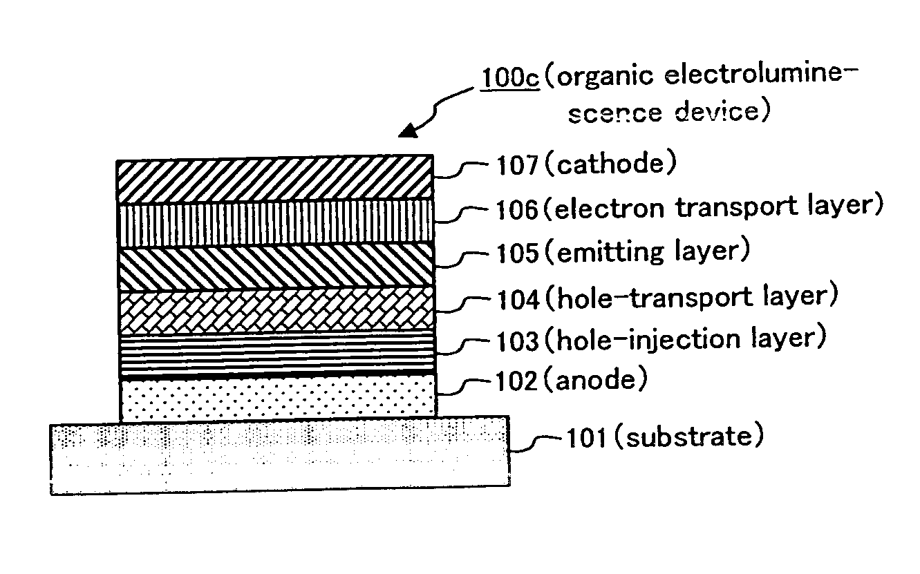
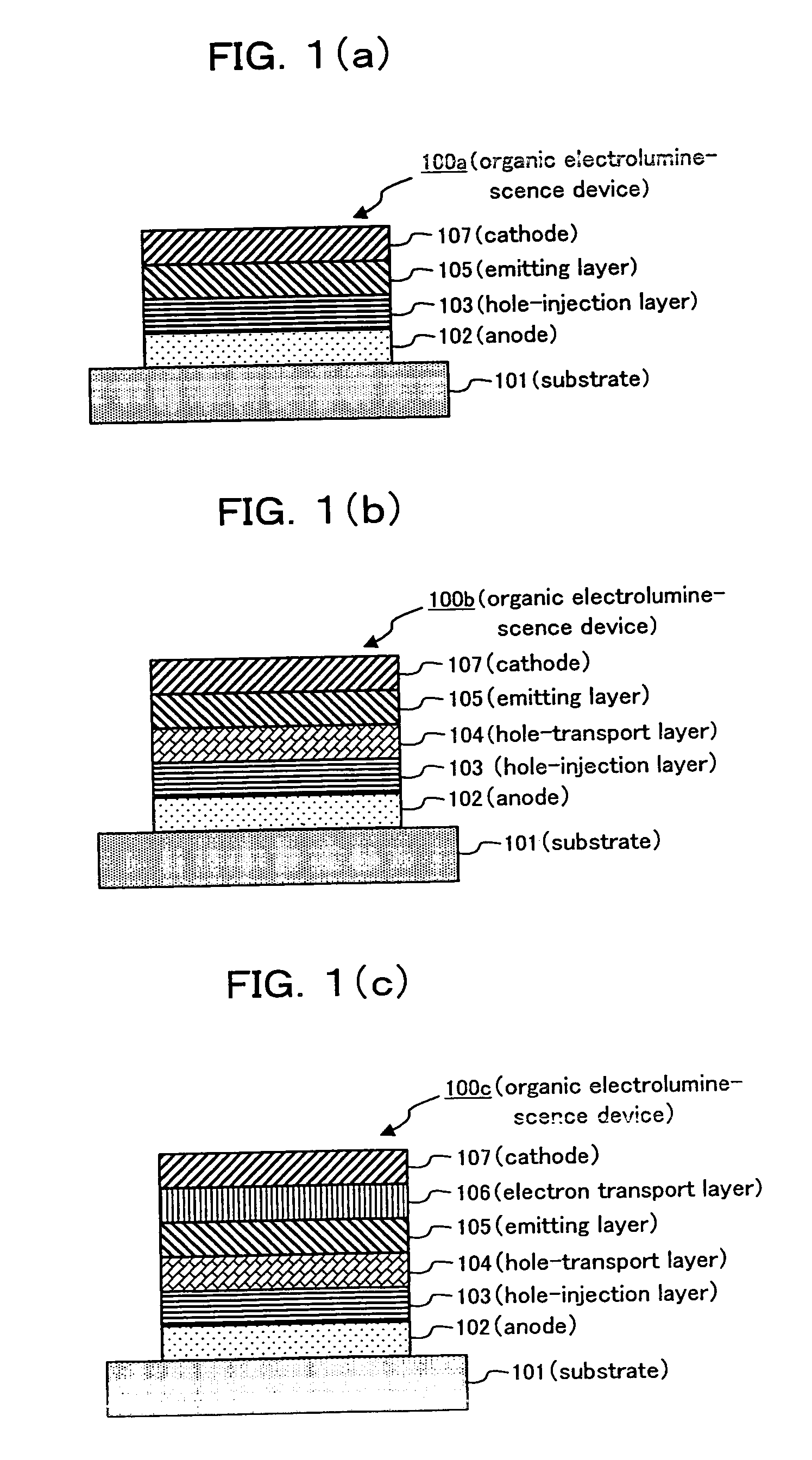
[0290] An organic electroluminescence device having a layer composition similar to that of organic electroluminescence device 100b, shown in FIG. 1(b), was prepared by the below-mentioned method.
[0291] A glass substrate, on which was deposited a transparent electricity conducting film of indium tin oxide (ITO) at a thickness of 120 nm (spatter film formation, Sanyo Vacuum Co.), was subjected to usual photolithography technique and hydrogen chloride etching, leading to a stripe pattern formation of 2 mm in width, so that an anode was prepared. This ITO substrate with pattern formation was washed, successively, with a detergent solution using ultrasonic, with extrapure water, with extrapure water using ultrasonic and again with extrapure water, followed by drying with compressed air and, finally, ultraviolet ray-ozone cleaning was conducted.
[0292] A composite mixture, comprising an ionic compound having a structure (A-1) shown in Table. 1, a charge transporting macromolecule compoun...
example 2
[0297] The same procedure as in Example 1 was followed except that compound (B-30) shown in the above-mentioned table was added at 0.2 weight % instead of ionic compound (A-1) as an ionic compound, and an organic electroluminescence device was prepared. The luminescence characteristics of the device obtained are shown in Table 15. It was possible to obtain a luminescence device functioning at a low voltage even at a heating / drying temperature of 200° C.
example 3
[0302] The same procedure as in Example 1 was followed to obtain an organic electroluminescence device except that a hole-injection layer was prepared under the conditions shown below.
TABLE 16Table 16SolventEthyl BenzoateConcentrationIonic Compound (compound0.40 Weight %of Coating(A-1) mentioned above as anSolutionexample)Charge Transporting0.33 Weight %Macromolecule Compound(compound (P-1) mentionedabove as an example)Charge Transporting1.67 Weight %Compound (compound (H-2)mentioned above as anexample)Revolution of1500 rpmSpinnerTime of30 SecondsRevolution ofSpinnerDrying230° C., 15 Minutes in Oven afterCondition80° C., 1 Minute on Hot Plate
[0303] The luminescence characteristics of the device obtained are shown in Table 20. As is apparent from the results in Table 20, it was possible to obtain a luminescence device functioning at a low voltage under heating / drying conditions of 230° C. for 15 minutes.
PUM
| Property | Measurement | Unit |
|---|---|---|
| temperature | aaaaa | aaaaa |
| current density | aaaaa | aaaaa |
| thickness | aaaaa | aaaaa |
Abstract
Description
Claims
Application Information


