
Magnetic random access memory

a random access and memory technology, applied in the field of integrated circuits, can solve the problems of not being able to operate the diode as simple, and achieve the effects of suppressing ‘joule heating’, low power consumption, and reduced active power

Inactive Publication Date: 2007-09-13
KIM JUHAN
View PDF0 Cites 25 Cited by
  • Summary
  • Abstract
  • Description
  • Claims
  • Application Information

AI Technical Summary

Benefits of technology

[0014]Removing MOS device from the memory cell, the cell structure is simplified, which enables to form the memory cell in between the routing metal layers, which can reduce cell area dramatically with no performance degradation. And the present invention can be implemented on the bulk and SOI wafer, which makes to integrate high density memory and control circuit on a chip, regardless of the process and fabrication facility. In doing so, it is more flexible to fabricate the memory chip, such that the process of the memory cell is independent of the MOS process. Hence, topping the memory cell is another fabrication facility which has prepared to deposit the dedicated material, after fabricating the base layers including the MOS transistors in a fabrication facility, because most of fabrication facilities provide the standard MOS transistor.
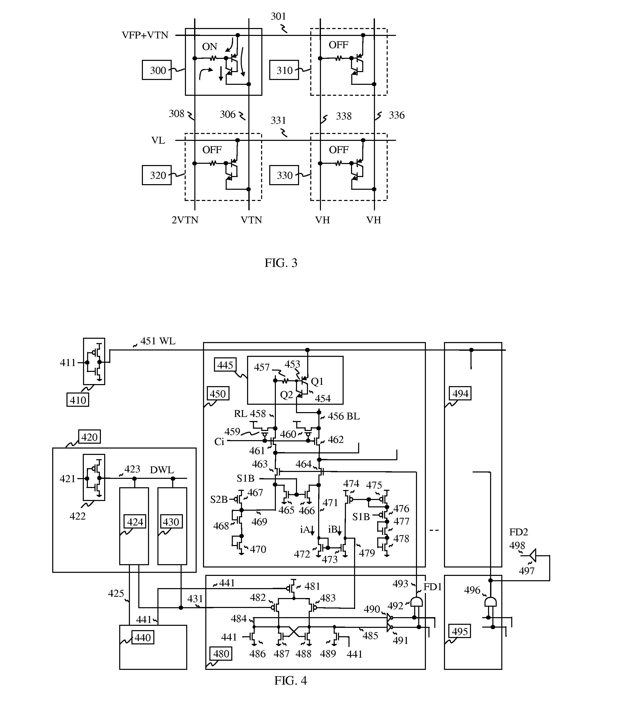
[0016]Low power consumption is realized, because the word line cuts off the holding current during standby. Thus there is no standby current in the memory cell. Active power is also reduced with self-closing data latch, wherein the latch output cuts off the bit line current after latching the stored data. Thus, low power consumption suppresses ‘Joule heating’, which may reduce gate delay and achieve high yield.
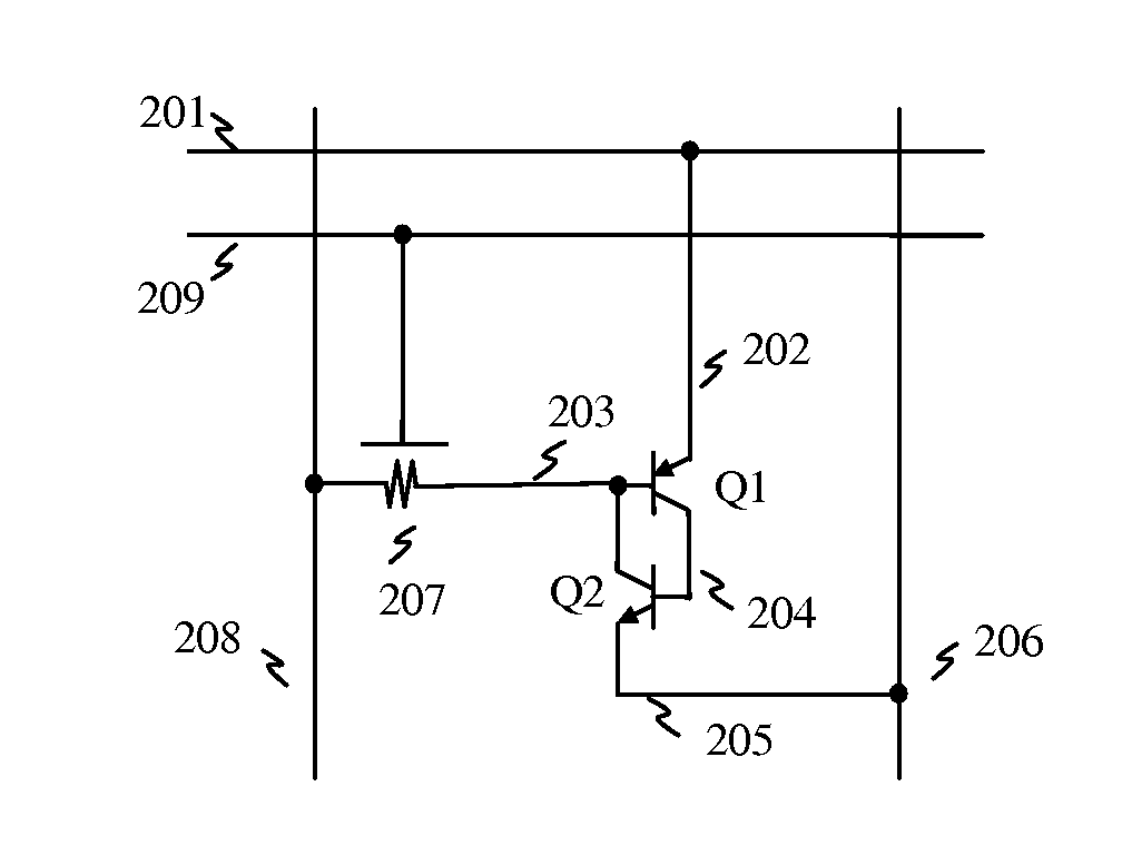
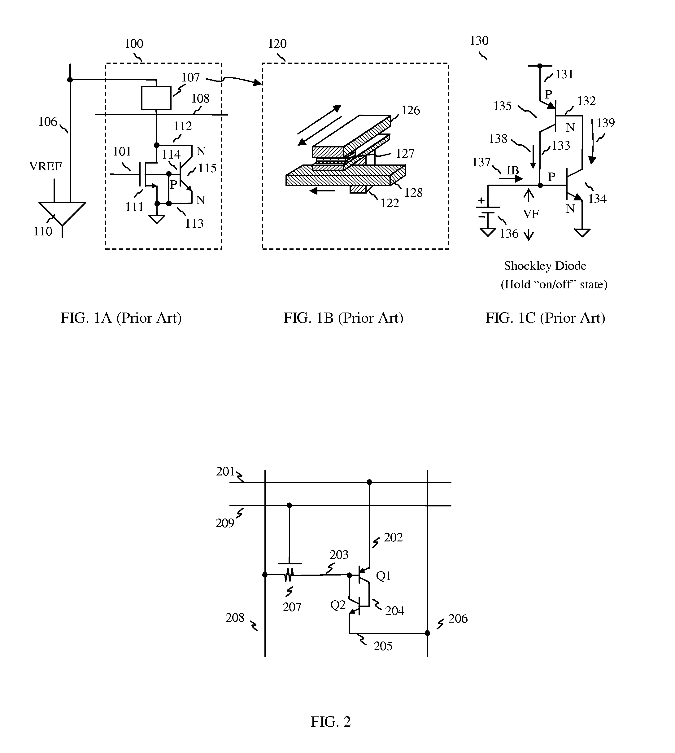
[0017]The memory operation is fast and stable. The diode output can be transferred to the bit line quickly, because the diode current is generally much higher than that of MOS transistor. The diode generates more current with its whole junction area while MOS transistor generates current with inversion layer on the surface. The four-terminal diode amplifies the read current from the word line to the bit line, wherein the storage element controls the base current when read. Thus the diode serves as a sense amplifier, which realizes more accurate sensing and also achieves fast access time. In the present invention, more flexible array architectures are introduced as well, in order to apply the magnetic memory array for the proper system applications. For the high density system, single memory cell stores a datum and two dummy cells generate reference voltage for sensing with slow access time. And for the low density and high speed system, dual memory cells store a datum, wherein one memory cell stores non-inverting data and another memory cell stores inverting data. Thus inverting data generates a reference voltage with no dummy cells and reduces access time with self-generating reference voltage. Hence, more accurate sensing is achieved because the magnetoresistive storage element has low magnetoresistance ratio (MR) ratio 20˜35% (0.2˜0.35 times) which is lower than that of other resistance storage element, such that phase change memory has around 100 times of the resistance difference between high data and low data.
[0018]The write driver circuit can be improved by using bipolar current mirror, which can flow more current, and occupy small area, compared to the MOS transistor driver circuit.

Problems solved by technology

However the operation of the diode is not as simple as that of MOS transistor because it has internal feedback loop and unidirectional current control in nature even though it has almost no parasitic effects, as long as punch-through is simply avoided in the base region with optimal length.

Method used


Image

  • Magnetic random access memory
  • Magnetic random access memory
  • Magnetic random access memory

Examples


Embodiment Construction

)

[0033]Reference is made in detail to the preferred embodiments of the invention. While the invention is described in conjunction with the preferred embodiments, the invention is not intended to be limited by these preferred embodiments. On the contrary, the invention is intended to cover alternatives, modifications and equivalents, which may be included within the spirit and scope of the invention as defined by the appended claims. Furthermore, in the following detailed description of the invention, numerous specific details are set forth in order to provide a thorough understanding of the invention. However, as is obvious to one ordinarily skilled in the art, the invention may be practiced without these specific details. In other instances, well-known methods, procedures, components, and circuits have not been described in detail so that aspects of the invention will not be obscured.

[0034]Detailed descriptions for the present invention are described as follows, which include the s...


PUM


Abstract

A magnetic memory includes a diode as an access device instead of MOS transistor and a magnetoresistive storage serves as a storage element, wherein the diode has four terminals, the first terminal is connected to a read word line, the second terminal serves as a storage node, the third terminal is floating, the fourth terminal is connected to a bit line, and wherein the magnetoresistive storage includes MTJ (magnetic tunnel junction) stack, the first electrode of the stack is connected to the storage node, the second electrode of the stack is connected to a free magnetic layer which serves as a resistor line, those electrodes are isolated by insulation layer, and the stack is coupled to a pinned magnetic layer which serves as a write word line. The diode also serves as a current amplifier with controlling the storage node through the storage element when the resistor line is asserted to measure the resistance of the storage element during read. And current-to-voltage converter receives the current output of the current amplifier, and transfers voltage output to the sense amp which amplifies the received voltage from the (main) memory cell and the reference voltage from the dummy memory cell(s). After latching data, the sense amp output cuts off the current path of the bit line. In the present invention, the memory cells are formed in between the routing layers. Hence the memory cells can be stacked over the peripheral circuits and alternatively multiple cells can be stacked.

Description

FIELD OF THE INVENTION[0001]The present invention relates generally to integrated circuits, in particular to the MRAM (Magnetic Random Access Memory).BACKGROUND OF THE INVENTION[0002]With conventional MOS (Metal-Oxide Semiconductor) access transistor approaching their speed and scaling limits, four-terminal the diode can replace MOS transistor as an access device for the next-generation memories. In the present invention, the diode serves as an access device for MRAM (Magnetic Random Access Memory or Magnetoresistive Random Access memory). Four-terminal the diode is more flexible than two-terminal the diode, three-terminal bipolar transistor or three-terminal MOS transistor (body is biased to the constant voltage), in order to control the magnetic memory such that the four-terminal the diode is used for read operation, and three-terminal bipolar transistor is used for write operation respectively. Furthermore, the diode serves as a sense amplifier when read. In addition, the bipolar...

Claims


Application Information

Patent Timeline
IPC IPC(8): G11C11/00
CPCG11C11/16H10B61/20
Inventor KIM, JUHAN
Owner KIM JUHAN
Learn More