Use of pi-conjugated organoboron polymers in thin-film organic polymer electronic devices

a technology of organoboron and organoboron polymer, which is applied in the direction of solid-state devices, discharge tubes/lamp details, natural mineral layered products, etc., can solve the problems of difficult design of electron-deficient conjugated polymer systems, poor properties of current n-type semi-conducting polymers, and unstable other icps in their semi-conducting state, etc., to reduce the electron-deficiency of polymers, improve the properties, and the aromatic units

Inactive Publication Date: 2007-09-20
TDA RES
View PDF16 Cites 45 Cited by
  • Summary
  • Abstract
  • Description
  • Claims
  • Application Information

AI Technical Summary

Benefits of technology

[0025] Novel polymers of this invention also include structures E, F, G, H, and I of Scheme 2. Representative synthetic methods of these novel polymers are given in Example 7. These novel polymers can provide improved properties compared to known polymers because of the higher electron deficiency of the aromatic unit.
[0026] Methods or improved methods for synthesis of certain pi-conjugated organoboron polymers are also provided. A significant improvement of the method of preparation of poly(arylborane)s polymers 3a-3e ove

Problems solved by technology

Some ICPs function as semiconducting polymers in their undoped state, however other ICPs are not stable in their semiconducting state.
In contrast, it is more difficult to design electron-deficient conjugated polymer systems.
Unfortunately, current n-type semiconducting polymers have generally poor properties, including low charge carrier density and low carrier mobility.
Furthermore, most of these materials are difficult to process, and some of them are difficult to synthesize.
The disadvantage of these non-polymeric semiconducting species is the low ch

Method used


Image

  • Use of pi-conjugated organoboron polymers in thin-film organic polymer electronic devices
  • Use of pi-conjugated organoboron polymers in thin-film organic polymer electronic devices
  • Use of pi-conjugated organoboron polymers in thin-film organic polymer electronic devices

Examples


example 1

Synthesis of Poly(arylboranes)

[0104] Poly(arylborane)s were prepared in a two-step synthesis from commercially available starting materials according as illustrated in Scheme 3; first two different borane reagents were prepared with a mesityl or tripyl group (step A), then the borane reagent was polymerized with an aromatic dibromo compound after transforming it into its Grignard reagent (step B). Representative syntheses are given below.

[0105] Scheme 4 shows the structure of the polymers prepared in this way, six with mesityl substituents on the boron atoms (x series) and seven with tripyl substituents (y series). Seven different dibromo-aromatic compounds were used as the starting materials: 5,5′-dibromobithiophene (polymers 3a), 2,5-dibromo-3-hexyl-thiophene (polymers 3b), 1,4-dibromo-2,5-bis(decyloxy)benzene (polymers 3c), 9,9-dihexyl-2,7-dibromofluorene (polymers 3d), 9,9-didodecyl-2,7-dibromofluorene (polymers 3e), 2,5-dibromo-3-dodecyl-thiophene (polymers 3f), and 9,9-diiso...

example 2

Synthesis of Poly(vinylborane)s

[0114] Poly(vinylborane)s were synthesized by reacting trans-1,2-bis(tributyltin)ethene with dichloroboranes (Scheme 5). 1H-NMR and elemental analysis indicated that the desired products were formed.

Synthesis of trans-1,2-bis(tributyltin)ethene

[0115] Tribuytyltin hydride (3.15 g, 10.8 mmol) and ethynyltributylstannane (3.4 g 10.8 mmol) and a catalytic amount of azobisisobutyronitrile (AIBN) were heated at 90° C. for 10 hours under an inert argon atmosphere. The reaction was vacuum distilled and the product was obtained in 95% yield.

Synthesis of Dichlorohexylborane

[0116] A solution of 1.91 g (16.25 mmol) of boron trichloride and 1.37 g (2.03 mL, 16.25 mmol) of 1-hexene in 5 cm3 of pentane was stirred under argon at −78° C. for 15 minutes. Tributylsilane (3.26 g, 16.25 mmol) was added dropwise to the stirred reaction mixture and left to stir overnight at room temperature. Vacuum distillation yielded dichlorohexylborane in 90% yield.

Synthesis of 3i...

example 3

Electrochemical Doping

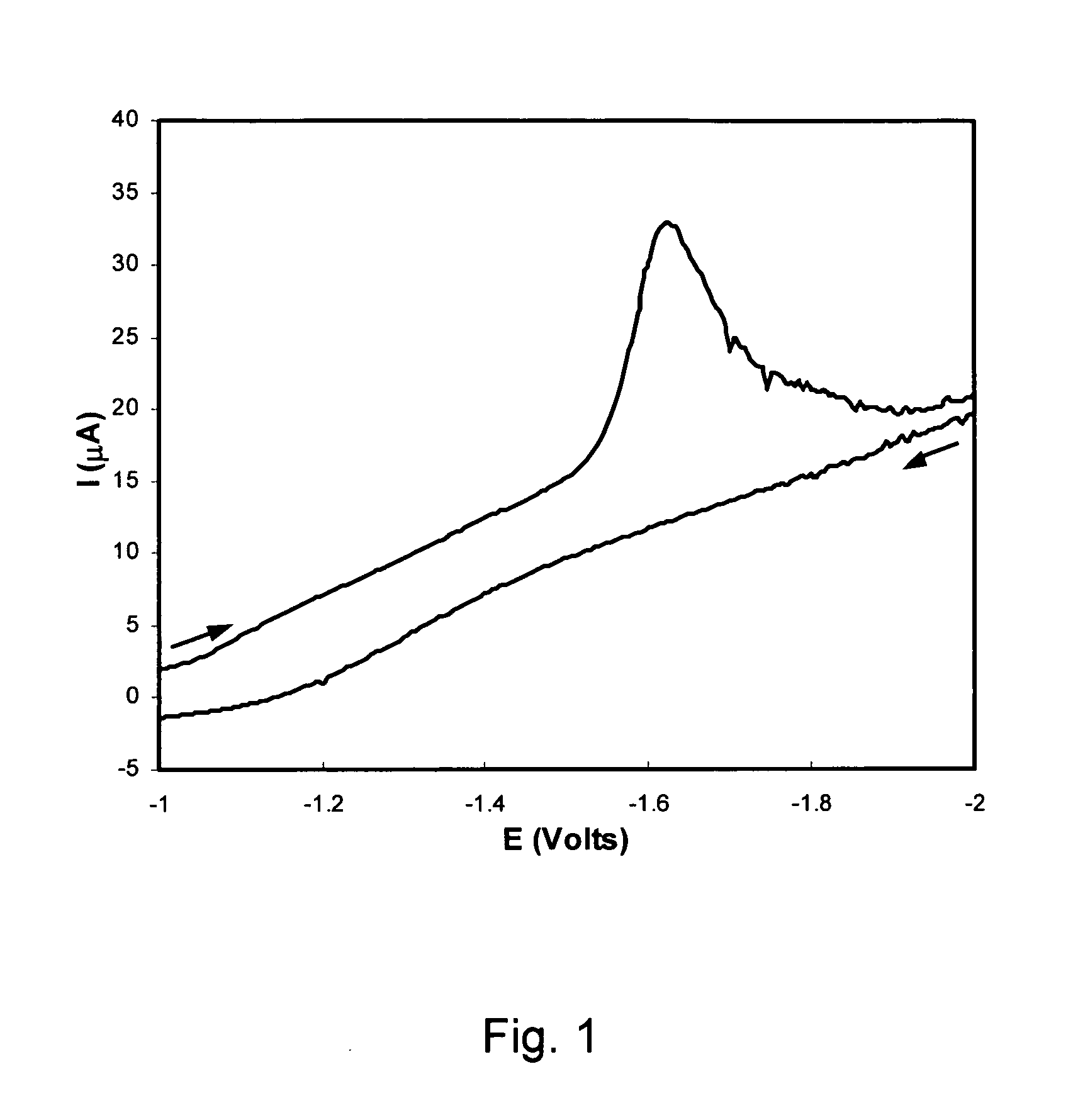
[0118] To identify the n-type semiconducting behavior of these polymers, we cast thin films onto a platinum working electrode and subjected these films to cyclic voltammetry. FIG. 1 shows the reduction of the 3ay polymer under an argon atmosphere. N-type behavior is generally indicated by a facile reduction process (electron injection) of the film on the electrode surface. We observe a reduction process in our materials, however, this reduced or n-doped form of the material is unstable or highly soluble because no film remains on the electrode after reducing the film.


PUM

PropertyMeasurementUnit
Lengthaaaaaaaaaa
Thicknessaaaaaaaaaa
Dielectric polarization enthalpyaaaaaaaaaa

Abstract

Pi-conjugated organoboron polymers for use in thin-film organic polymer electronic devices. The polymers contain aromatic and or unsaturated repeat units and boron atoms. The vacant p-orbital of the boron atoms conjugate with the pi-conjugated orbital system of the aromatic or unsaturated monomer units extending the pi-conjugation length of the polymer across the boron atoms. The pi-conjugated organoboron polymers are electron-deficient and, therefore, exhibit n-type semiconducting properties, photoluminescence, and electroluminescence. The invention provides thin-film organic polymer electronic devices, such as organic photovoltaic cells (OPVs), organic diodes, organic photodiodes, organic thin-film transistors (TFTs), organic field-effect transistors (OFETs), printable or flexible electronics, such as radio-frequency identification (RFID) tags, electronic papers, and printed circuit elements, organic light-emitting diodes (OLEDs), polymer light-emitting diodes (PLEDs), and energy storage devices employing the pi-conjugated organoboron polymers. In OLED and PLED applications these materials are used as the electron transport layer (ETL) to improve device efficiency. The polymers which exhibit photo- and electroluminescence are also useful as light-emitting material in PLEDs.

Description

STATEMENT REGARDING FEDERALLY SPONSORED RESEARCH OR DEVELOPMENT [0001] This invention was made, at least in part, with funding from National Science Foundation contract DMI-0319320. The United States government has certain rights in the invention.FIELD OF THE INVENTION [0002] This invention relates to the use of pi-conjugated (or π-conjugated) organoboron polymers in thin film electronic devices and methods for the fabrication of such devices. BACKGROUND OF THE INVENTION [0003] The specific functions of many electronic components and devices arise from the unique interactions existing between p-type and n-type conducting and semiconducting materials. Until a few years ago, inorganic conductors and semiconductors entirely dominated the electronic industry. In recent years there has been a major worldwide research effort to develop conducting and semiconducting organic compounds and polymers, and to use them to fabricate plastic electronic devices, such as organic thin film transistor...

Claims


Application Information

Patent Timeline
IPC IPC(8): H01L51/00H01L51/54C08G79/08
CPCC08G79/08Y10S428/917C09K11/06C09K2211/1425C09K2211/1433C09K2211/1466C09K2211/1475C09K2211/1483H01L51/0035H01L51/0039H01L51/004H01L51/0043H01L51/008H01L51/0541H01L51/0545H01L51/4246H01L51/4253H01L51/5012H05B33/14Y02E10/549C08G2261/94H10K85/141H10K85/115H10K85/111H10K85/151H10K85/322H10K10/464H10K30/211H10K10/466H10K30/30H10K50/11
Inventor LUEBBEN, SILVIA DEVITOSAPP, SHAWN A.
Owner TDA RES
Why Eureka
Try Eureka